
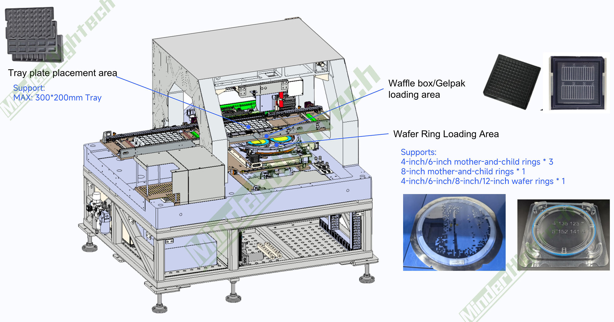
Die Thickness Minimum :50um (Thinner Pending Discuss ) Ultra Thin Die Sorter MDND-120UT Project Parameters Equipment Name MDND-120UT multi-function die bonder Equipment Model MDND-120UT Bonding Accuracy/Angle ±20um, ...
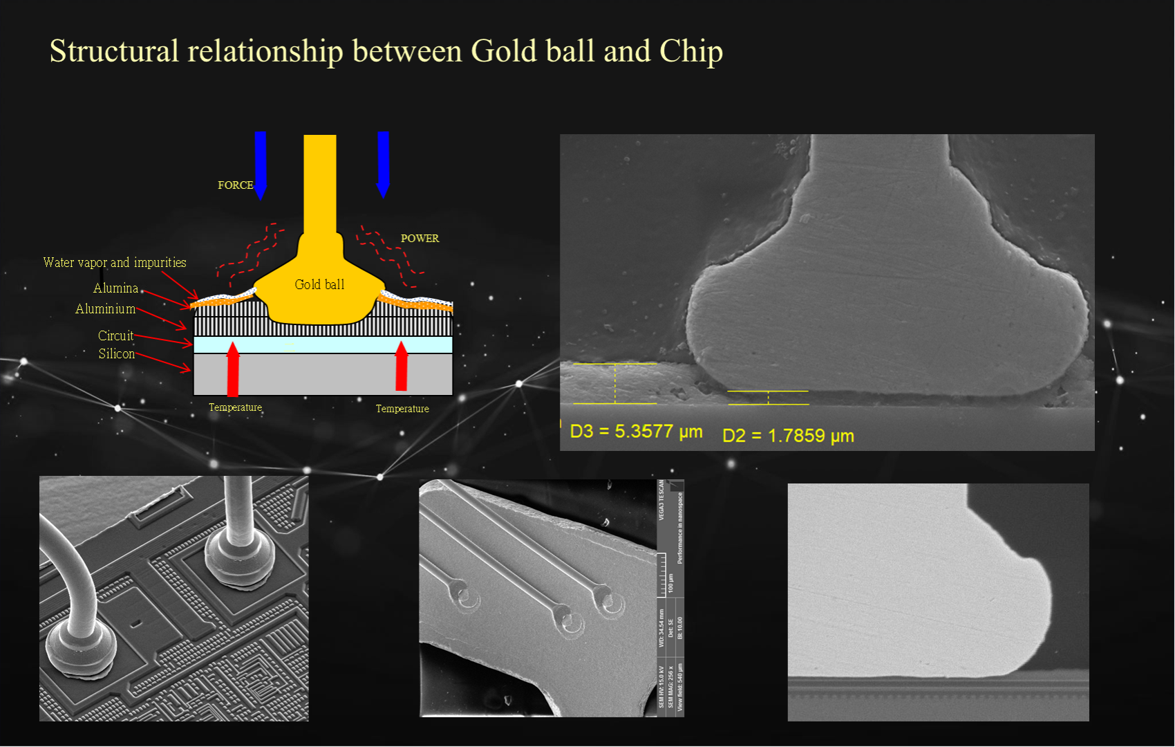
Basic Theory of Fully Automatic Semiconductor Wire Ball Bonding Machine
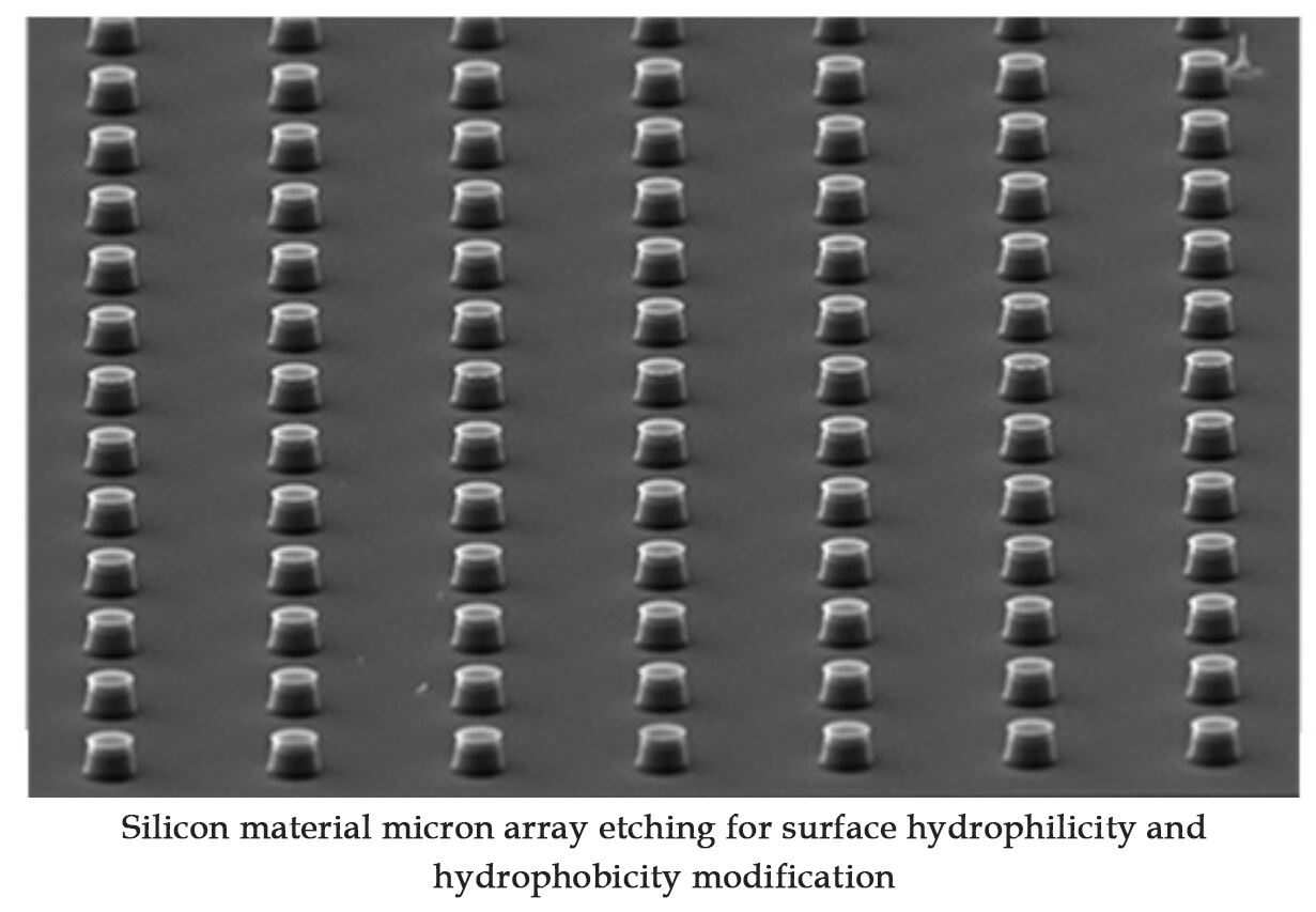
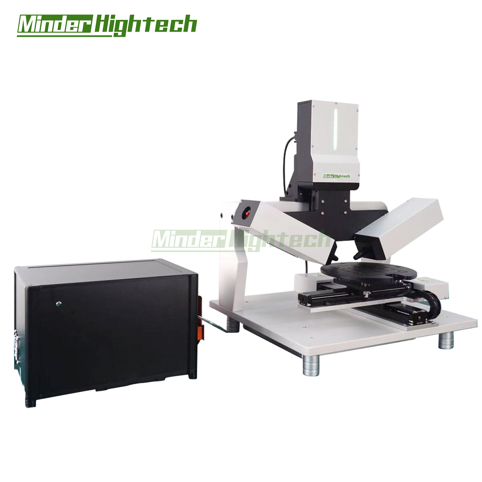
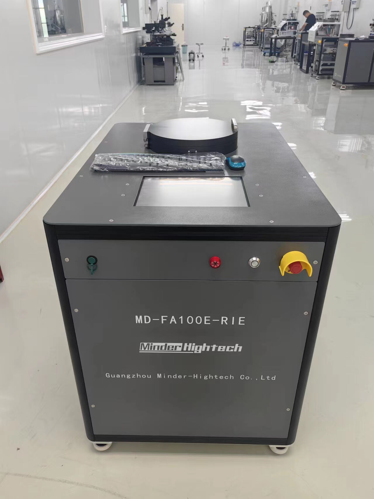
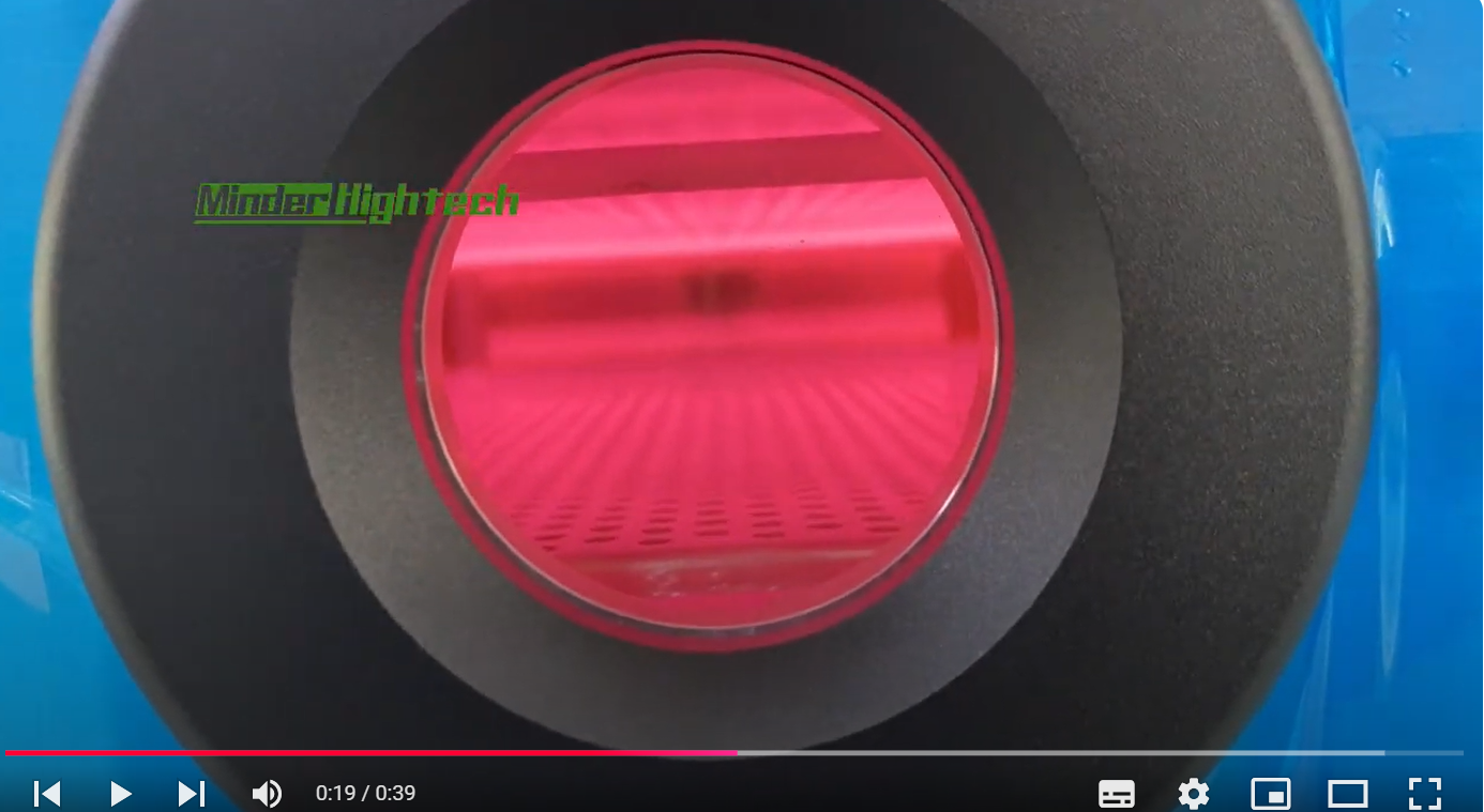
Semiconductor Manufacturing / Plasma Etching / Reactive Ion Etching
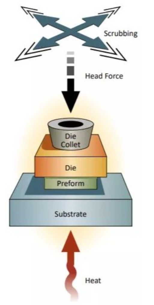
Eutectic refers to the phenomenon of eutectic fusion in eutectic solder at relatively low temperatures. Eutectic alloys directly change from solid to liquid without going through the plastic stage, and their thermal conductivity, resistance, shear fo...
IC design, also known as integrated circuit design, has high precision in nano process technology, and the higher the accuracy, the more advanced the production process. When more transistors are integrated into the processor, the chip can achieve mo...
Low dimensional material etching refers to the process of etching two-dimensional materials (such as graphene, molybdenum disulfide, etc.) and one-dimensional materials (such as nanowires, nanotubes, etc.). The purpose of low dimensional material etc...
Vacuum Plasma and Microwave Plasma Application: Semiconductor industry Car industry Mobile industry Camera module PCB industry LED industry FPC industry Material industry Metal industry Ceramics industry
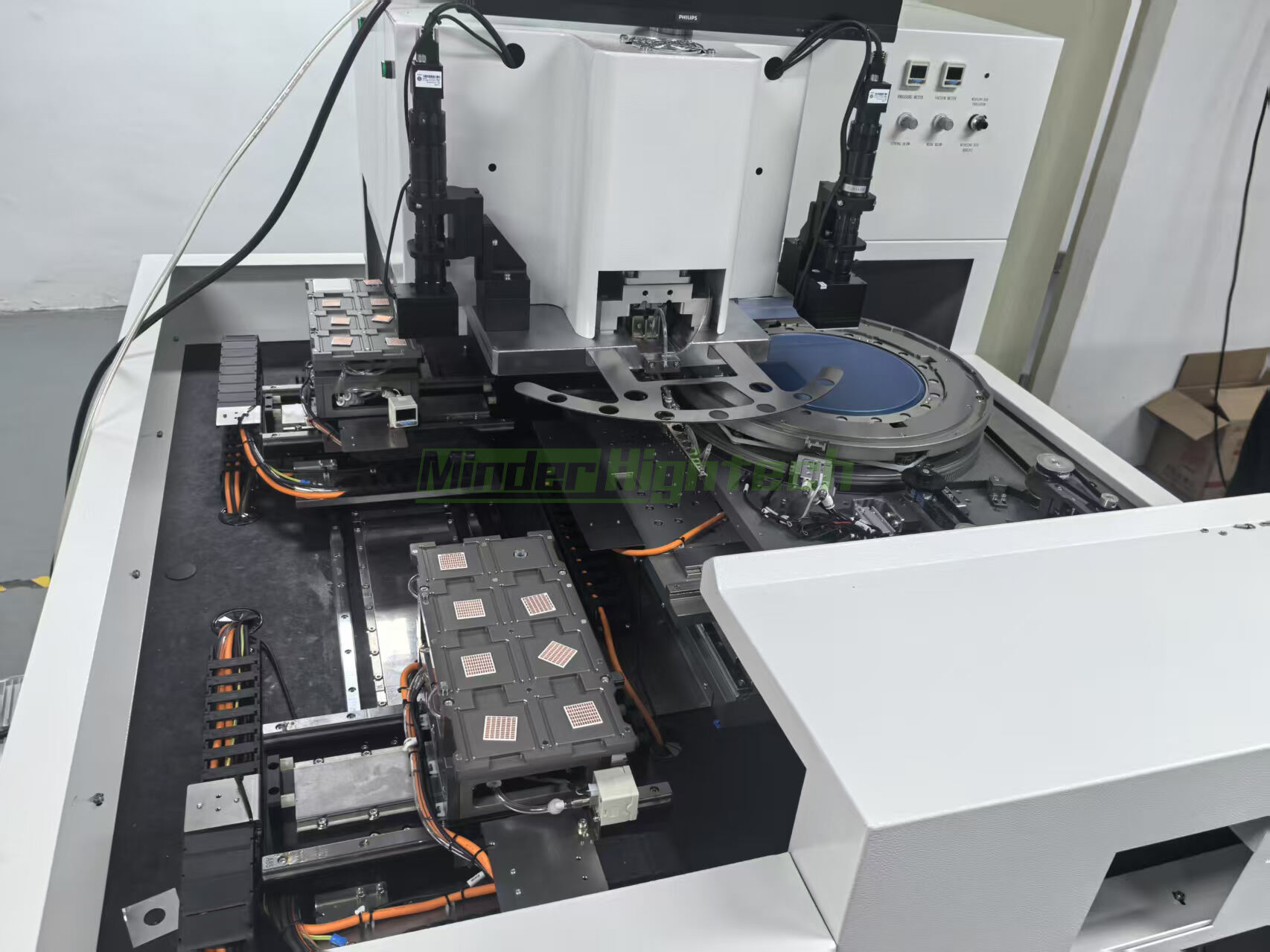
Semiconductor TEC TEC Thermoelectric Cooler / Thermo Electric Cooler Die bonding machine
A customer from Brazil who makes display screen casings discovered during R&D that their products were peeling off after glue was dispensed. After communicating with MH engineers, we customized this equipment solution for them: direct injection p...
Guangzhou Minder-Hightech Co.,Ltd.
Copyright © Guangzhou Minder-Hightech Co.,Ltd. All Rights Reserved
 EN
EN
 AR
AR
 BG
BG
 CS
CS
 DA
DA
 NL
NL
 FI
FI
 FR
FR
 DE
DE
 EL
EL
 IT
IT
 KO
KO
 NO
NO
 PL
PL
 PT
PT
 RO
RO
 RU
RU
 ES
ES
 SV
SV
 TL
TL
 IW
IW
 ID
ID
 LT
LT
 SR
SR
 SL
SL
 UK
UK
 VI
VI
 ET
ET
 HU
HU
 TH
TH
 TR
TR
 FA
FA
 AF
AF
 MS
MS
 GA
GA
 IS
IS
 HY
HY
 AZ
AZ
 KA
KA


