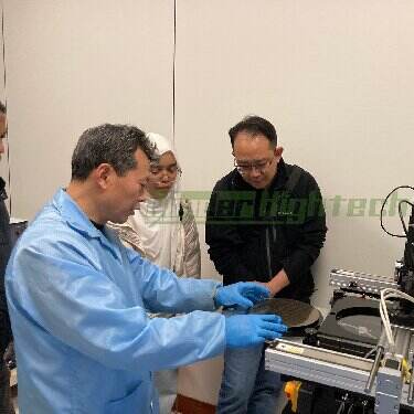
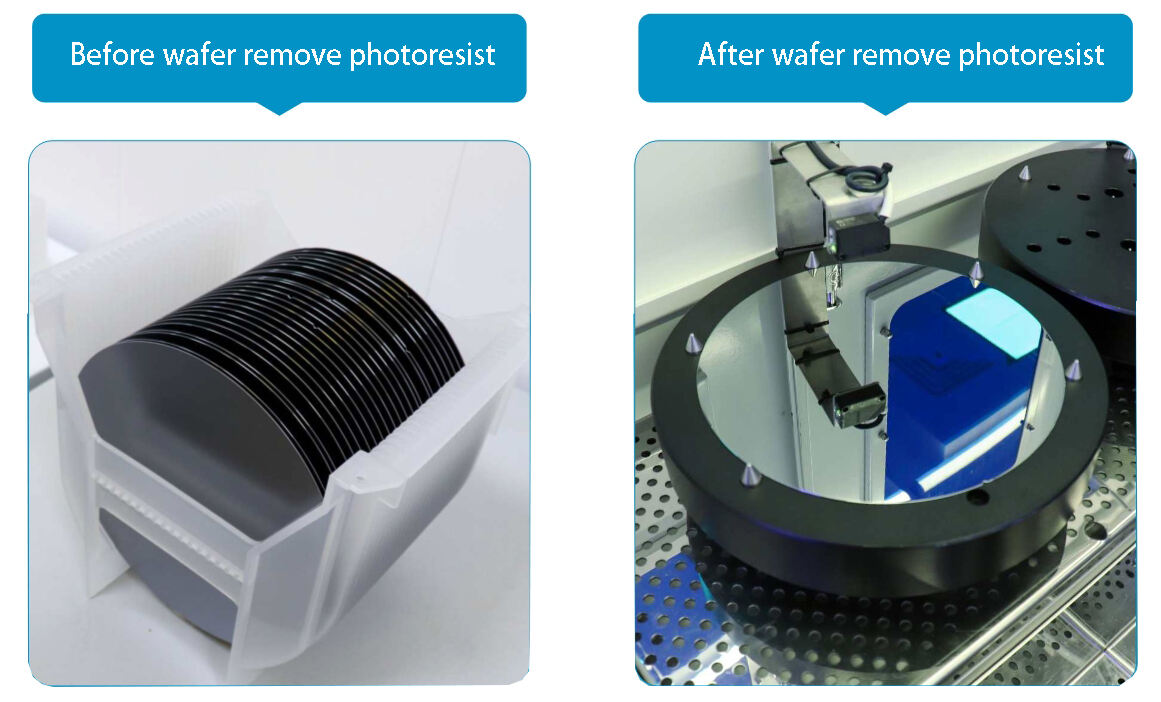
This device is highly suitable for use in university chip laboratories. We provide you with one-stop professional solution for semiconductor fabrication and various chips package equipments sulotion from China. The process engineer and electrical engineer from the user side have completed the acceptance inspection of the Mask Aligner -MDXN-G33D8 equipment.
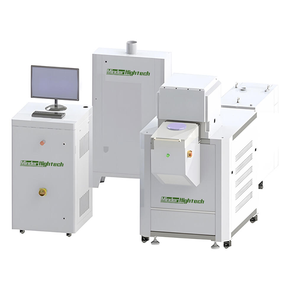
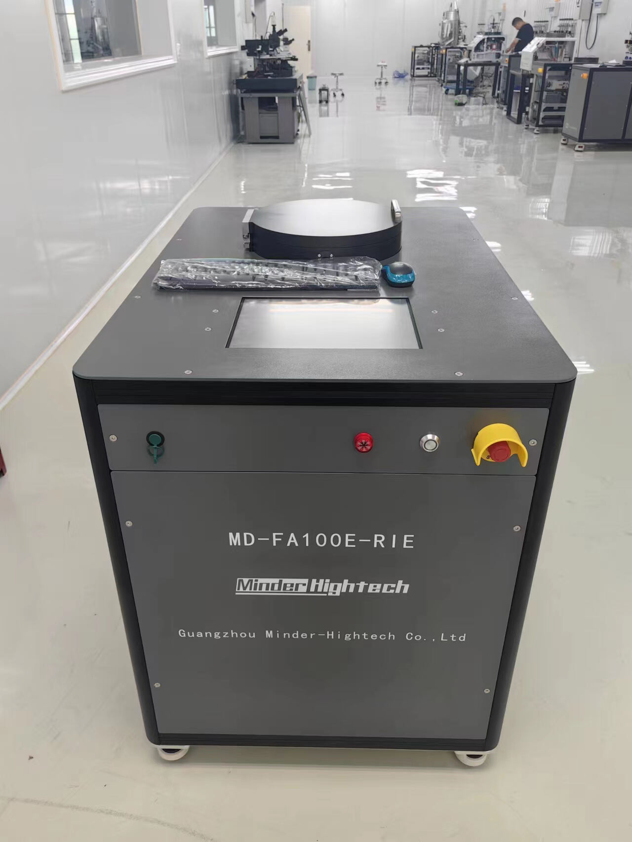
Semiconductor Manufacturing / Plasma Etching / Reactive Ion Etching
IC design, also known as integrated circuit design, has high precision in nano process technology, and the higher the accuracy, the more advanced the production process. When more transistors are integrated into the processor, the chip can achieve mo...
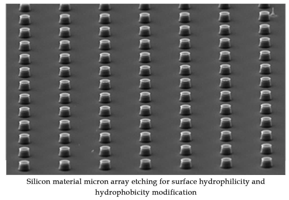
Low dimensional material etching refers to the process of etching two-dimensional materials (such as graphene, molybdenum disulfide, etc.) and one-dimensional materials (such as nanowires, nanotubes, etc.). The purpose of low dimensional material etc...
The rapid annealing furnace uses halogen infrared lamp as the heat source to heat the material to the required temperature through rapid heating, so as to improve the crystal structure and optoelectronic properties of the material. Its features inc...
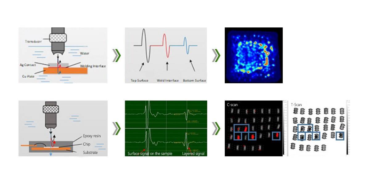
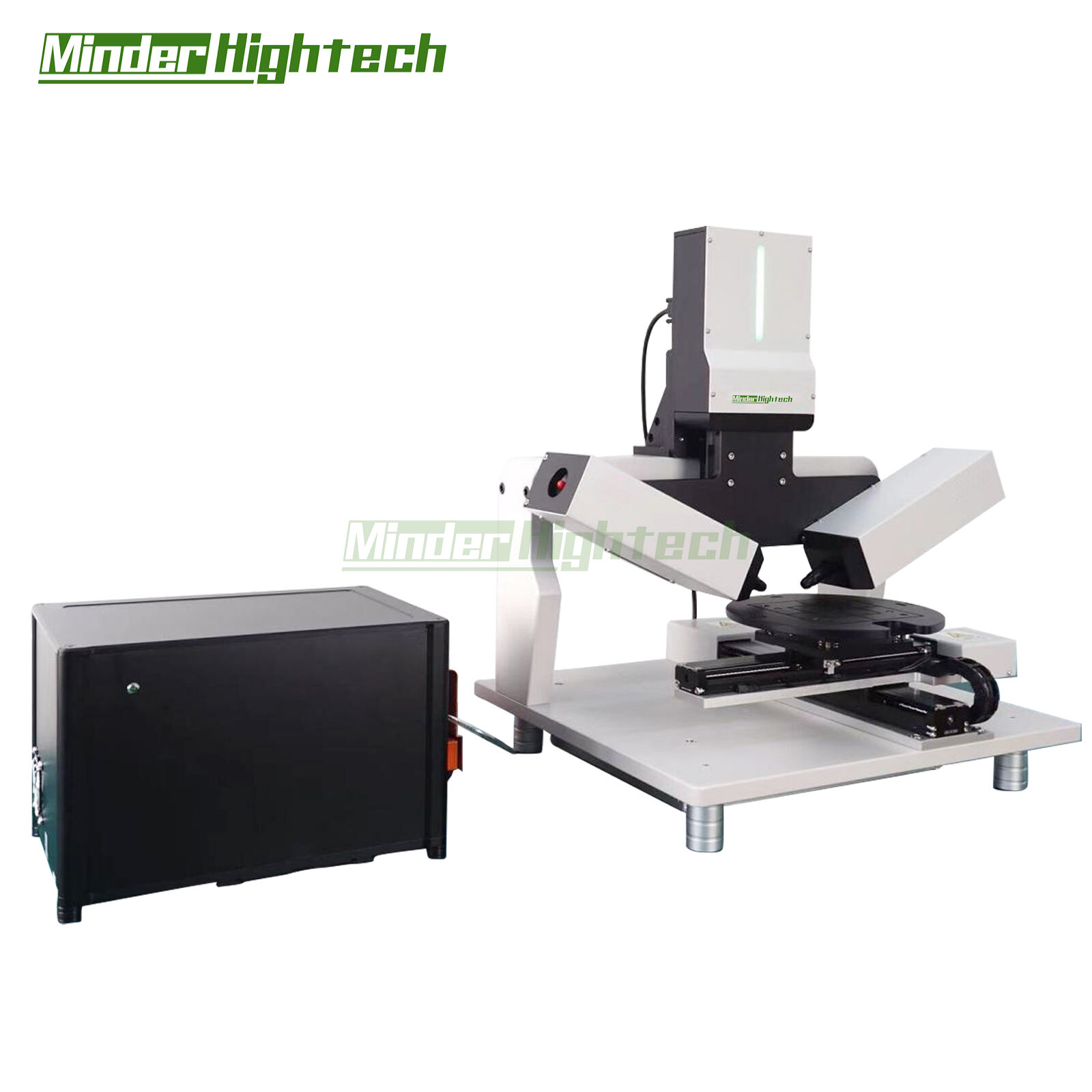
Provides flexibility for your production and laboratory departments. Provide high-quality FA Lab functionality for semiconductor facilities. Categories: Electrical & Electronics, Inspection, Test & Measurement Equipment, OKOS, Scanning Acoustic Microscope (SAM), Semiconductor.
Guangzhou Minder-Hightech Co.,Ltd.
Copyright © Guangzhou Minder-Hightech Co.,Ltd. All Rights Reserved
 EN
EN
 AR
AR
 BG
BG
 CS
CS
 DA
DA
 NL
NL
 FI
FI
 FR
FR
 DE
DE
 EL
EL
 IT
IT
 KO
KO
 NO
NO
 PL
PL
 PT
PT
 RO
RO
 RU
RU
 ES
ES
 SV
SV
 TL
TL
 IW
IW
 ID
ID
 LT
LT
 SR
SR
 SL
SL
 UK
UK
 VI
VI
 ET
ET
 HU
HU
 TH
TH
 TR
TR
 FA
FA
 AF
AF
 MS
MS
 GA
GA
 IS
IS
 HY
HY
 AZ
AZ
 KA
KA


