Etching: A key process for semiconductor patterning, its importance is highlighted.
Etching is the core process of semiconductor patterning, and the etcher is regarded as one of the three core devices in semiconductor manufacturing. Etching equipment is mainly used to remove materials in specific areas to form tiny structural patterns. It is known as one of the three core devices in semiconductor manufacturing along with photolithography and thin film deposition, and its importance is prominent and its status is crucial.
Etching equipment: Dry etching is the main method, with ICP and CCP equally divided
Etching can be divided into wet etching and dry etching. Wet etching has poor anisotropy, and the sidewall is prone to lateral etching, resulting in etching deviation. It is usually used for applications with larger process sizes. Dry etching is the current mainstream etching technology, among which plasma dry etching is the most widely used.
Depending on the plasma generation method, plasma etching is divided into two categories: ICP (inductive plasma etching) and CCP (capacitive plasma etching). ICP is mainly used for silicon, metal and some dielectric etching, while CCP is mainly used for dielectric etching. According to Gartner data, in 2022, in the global etching equipment market, ICP and CCP will have a market share of 47.9% and 47.5% respectively, with a total market share of 95.4%, which is the mainstream of etching equipment.
Trend: Atomic Layer Etching (ALE)
Traditional plasma etching equipment faces a series of challenges such as etching damage, load effect and control accuracy, while atomic layer etching (ALE) can achieve precise etching at the single atomic level and is an effective solution. ALE can be regarded as a mirror process of ALD. Its principle is: 1) Introducing the binding gas into the etching chamber and adsorbing it on the surface of the material to form a binding layer. This is a modification step and has self-stopping properties; 2) Removing excess binding gas in the chamber, introducing etching gas to bombard the etching surface, removing the atomic-level binding layer, and exposing the unmodified surface. This is an etching step and also has self-stopping properties. After the above steps are completed, the single atomic layer film on the surface can be accurately removed.
The advantages of atomic layer deposition (ALE) include: 1) Directional etching can be achieved; 2) Equal amount of etching can be achieved even if the aspect ratio is different.
Etching equipment: one of the three core equipment, with a considerable market size.
As one of the three major equipment in semiconductor manufacturing, the etcher has a high value and a considerable market size. According to Gartner data, in 2022, etching equipment accounted for 22% of the value of semiconductor front-end equipment, ranking second only to thin film deposition equipment; in terms of market size, according to Mordor Intelligence data, in 2024, the global semiconductor etching equipment market size is expected to be US$23.80 billion, and by 2029 it is expected to grow to US$34.32 billion, with a CAGR of about 7.6% during the period, with a considerable market size and a rapid growth rate.
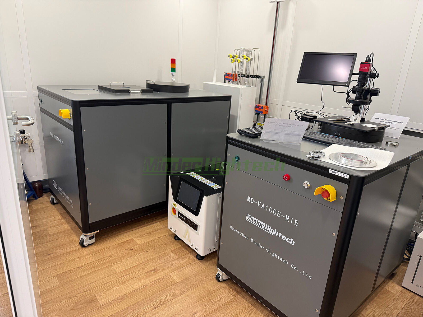
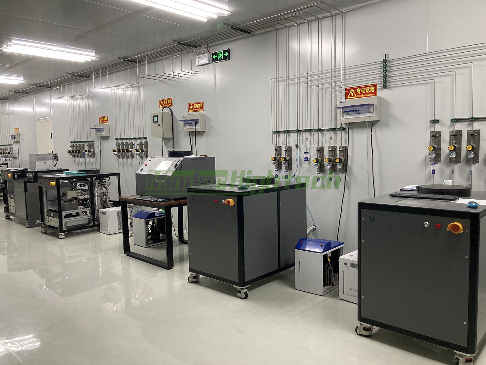
Guangzhou Minder-Hightech Co.,Ltd.
Copyright © Guangzhou Minder-Hightech Co.,Ltd. All Rights Reserved
 EN
EN
 AR
AR
 BG
BG
 CS
CS
 DA
DA
 NL
NL
 FI
FI
 FR
FR
 DE
DE
 EL
EL
 IT
IT
 KO
KO
 NO
NO
 PL
PL
 PT
PT
 RO
RO
 RU
RU
 ES
ES
 SV
SV
 TL
TL
 IW
IW
 ID
ID
 LT
LT
 SR
SR
 SL
SL
 UK
UK
 VI
VI
 ET
ET
 HU
HU
 TH
TH
 TR
TR
 FA
FA
 AF
AF
 MS
MS
 GA
GA
 IS
IS
 HY
HY
 AZ
AZ
 KA
KA


