Low dimensional material etching refers to the process of etching two-dimensional materials (such as graphene, molybdenum disulfide, etc.) and one-dimensional materials (such as nanowires, nanotubes, etc.). The purpose of low dimensional material etching is to prepare nanostructures with specific shapes and sizes, in order to achieve control and optimization of material properties and device performance. Low dimensional materials are generally etched using chemical etching methods. It uses chemical reactions to process materials, and commonly used chemical etching methods include wet etching and dry etching.
The difficulties in etching low dimensional materials mainly include: 1 Etching selection: Different low dimensional materials have different requirements for etching conditions, and suitable etching conditions need to be selected based on the specific properties of the material, such as etching gas, power, time, etc. 2. Etching quality: The etching quality of low dimensional materials directly affects their performance and applications, and it is necessary to control the etching rate and depth to avoid excessive or insufficient etching. 3. Etching uniformity: The etching uniformity of low dimensional materials is crucial for preparing high-quality devices, and it is necessary to control parameters such as temperature, gas flow rate, and pressure during the etching process to ensure etching uniformity. 4. Post etching treatment: After etching, the sample needs to be cleaned and treated to remove etching products and residual etching gases, ensuring the surface quality and stability of the sample.
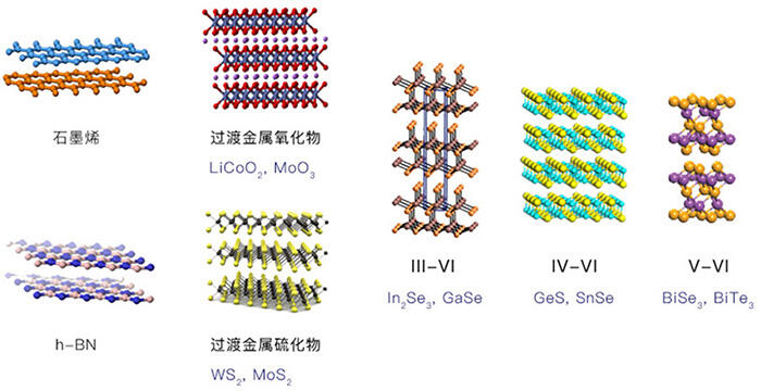
Two dimensional electronic thin film materials refer to new two-dimensional materials with single or few atomic layer thicknesses mainly formed by covalent bonding.
Mainly includes:
1. Graphene ,h-BN;
2. Transition metal oxides;
3. TMCs,MX2(M=Mo, W, Re, Ti, Zr, Hf, V, Nb, Ta, Pt, Pd, Fe; X=S, Se, Te),MoS2、WS2;etc.
4. Partial III/IV/V sulfur based materials, etc.
Early research on two-dimensional electronic thin film materials, especially graphene materials, mainly focused on the preparation methods of two-dimensional materials, such as mechanical exfoliation, reduction, deposition, etc., as well as the study of material properties. With the continuous breakthroughs in the preparation of large-sized two-dimensional thin film materials, people have begun to turn their attention to the preparation of devices. The thinning and patterning of two-dimensional thin film materials are key to the preparation of two-dimensional devices. The traditional semiconductor plasma dry etching method has two fatal disadvantages in the thinning and patterning of two-dimensional materials:
1. Excessive etching rate cannot meet the precise and stable etching of 2D material atomic layers (sub nanometer level);
2. High energy ion bombardment can cause structural damage to 2D materials, resulting in material defects
The characteristics that a specialized etching machine for two-dimensional materials should possess are:
1. Control the output power at the milliwatt level;
2. The minimum starting power should be controlled below 5W;
3. Layer by layer etching control, with an etching rate that can be precisely controlled between 0.3 and 10 layers per minute
4. The ion energy for bombarding the sample can be as low as 10 eV or less
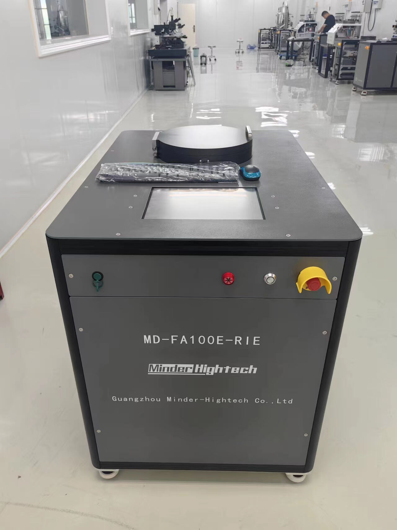
2D Material Etching Solution - SHL 100 μ/200 μ - RIE
We have developed the SHL 100 μ/200 μ - RIE series machine based on microplasma technology to address the application issues of two-dimensional material patterning mentioned above. The machine is used for layer reduction etching and patterned etching of two-dimensional materials such as graphene. Figure 2 shows the appearance of the two-dimensional material etching machine.
The main applications of two-dimensional material etching machines are:
1. 2D material delamination etching to prepare single-layer or few layer 2D material samples
2. 2D material pattern etching to prepare 2D material devices
3. 2D material modification processing
Core performance indicators of two-dimensional material etching machine:
1. Can handle samples up to four inches/eight inches and smaller in size;
2. Ultra weak plasma etching: It can achieve a process power as low as 3 W (@ 100mm electrode) RF (@ 13.56 MHz), with a power density as low as 38 mW/cm2 and an output power accuracy of less than 0.1 W;
3. The ion energy for bombarding the sample can be as low as 10 eV;
4. It can achieve stable and precise atomic layer etching from 0.1 layer/min to 1 layer/min;
The main configuration of the two-dimensional material etching machine is:
1. It can be configured with 3 to 8 process gases and digitally controlled with metal sealed MFC;
2. Using semiconductor grade 6061 aluminum as the process chamber material to eliminate contamination of the sample by impurity elements in stainless steel materials;
3. The load lock chamber can be configured, and the background vacuum of the process chamber can reach 4 x 10⁻⁴ Pa;
4. Fully automatic process control, graded user login management, real-time recording of comprehensive process data and machine status data, Recipe process library management and calling, component lifecycle management and fault self inspection.
2D material etching machine graphical results:
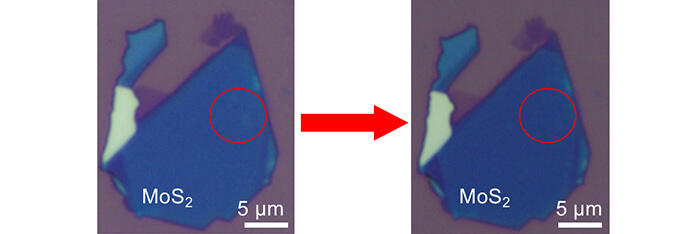
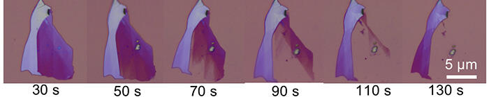
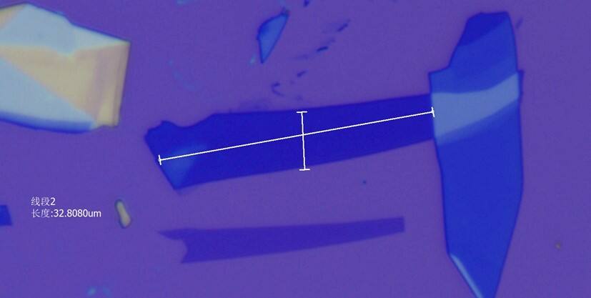
SHL100μ-RIE,38 mW/cm2, 10s: Clean residue on the surface of fewer layers flaked MoS2.
From Sun Jian & Liu Xiaochi Team, School of Physics and Electronics of Central South University.
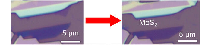
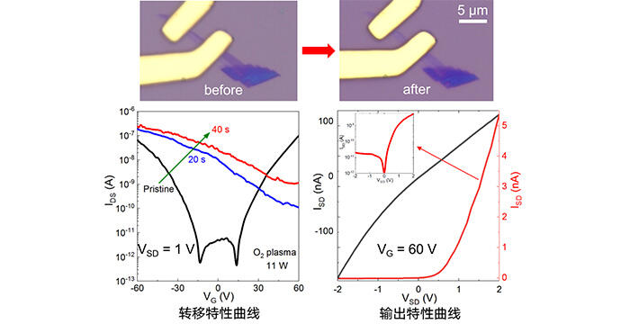
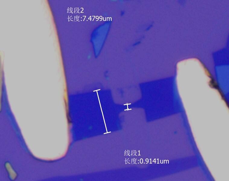
SHL100μ-RIE, 51 mW/cm2, 3s: Etch MoS2 layer-by-layer.
From Sun Jian & Liu Xiaochi Team, School of Physics and Electronics of Central South University.
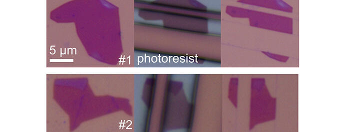
SHL100μ-RIE, 0.5 W/cm2: Etch Graphene layer-by-layer.
From Sun Jian & Liu Xiaochi Team, School of Physics and Electronics of Central South University.
SHL100μ-RIE, 140 mW/cm2: WSe2 p-Type doping.
From Sun Jian & Liu Xiaochi Team, School of Physics and Electronics of Central South University.
SHL100μ-RIE, 0.5 W/cm2: Etch Graphene layer-by-layer.
From Sun Jian & Liu Xiaochi Team, School of Physics and Electronics of Central South University.
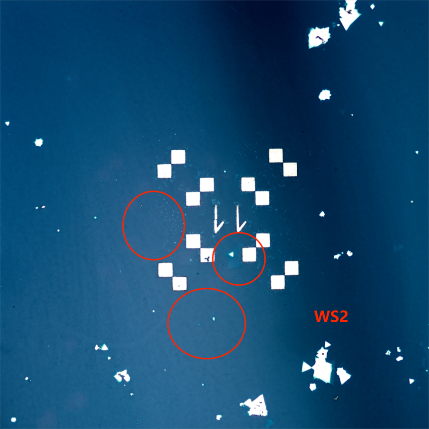
SHL100μ-RIE, Etch WS2 layer-by-layer.
From Xuefei Li Team, School of Huazhong University of Science and Technology.
SHL100μ-RIE, Etch Graphene layer-by-layer.
Guangzhou Minder-Hightech Co.,Ltd.
Copyright © Guangzhou Minder-Hightech Co.,Ltd. All Rights Reserved
 EN
EN
 AR
AR
 BG
BG
 CS
CS
 DA
DA
 NL
NL
 FI
FI
 FR
FR
 DE
DE
 EL
EL
 IT
IT
 KO
KO
 NO
NO
 PL
PL
 PT
PT
 RO
RO
 RU
RU
 ES
ES
 SV
SV
 TL
TL
 IW
IW
 ID
ID
 LT
LT
 SR
SR
 SL
SL
 UK
UK
 VI
VI
 ET
ET
 HU
HU
 TH
TH
 TR
TR
 FA
FA
 AF
AF
 MS
MS
 GA
GA
 IS
IS
 HY
HY
 AZ
AZ
 KA
KA


