Eutectic refers to the phenomenon of eutectic fusion in eutectic solder at relatively low temperatures. Eutectic alloys directly change from solid to liquid without going through the plastic stage, and their thermal conductivity, resistance, shear force, reliability, etc. are superior to traditional epoxy bonding.
Eutectic welding is widely used in the welding of high-frequency, high-power devices, and LED devices with high heat dissipation requirements due to its advantages of high welding strength, strong shear force, low connection resistance, and high heat transfer efficiency.
The conventional automatic surface mounting machine has a pressure control range of 10-250g, and can be programmed and controlled for each placement. It also has a real-time pressure feedback system, a pulse heating method, and a real-time temperature detection system. Raw material cleaning adopts UV ultraviolet cleaning machine and BT plasma cleaning machine.
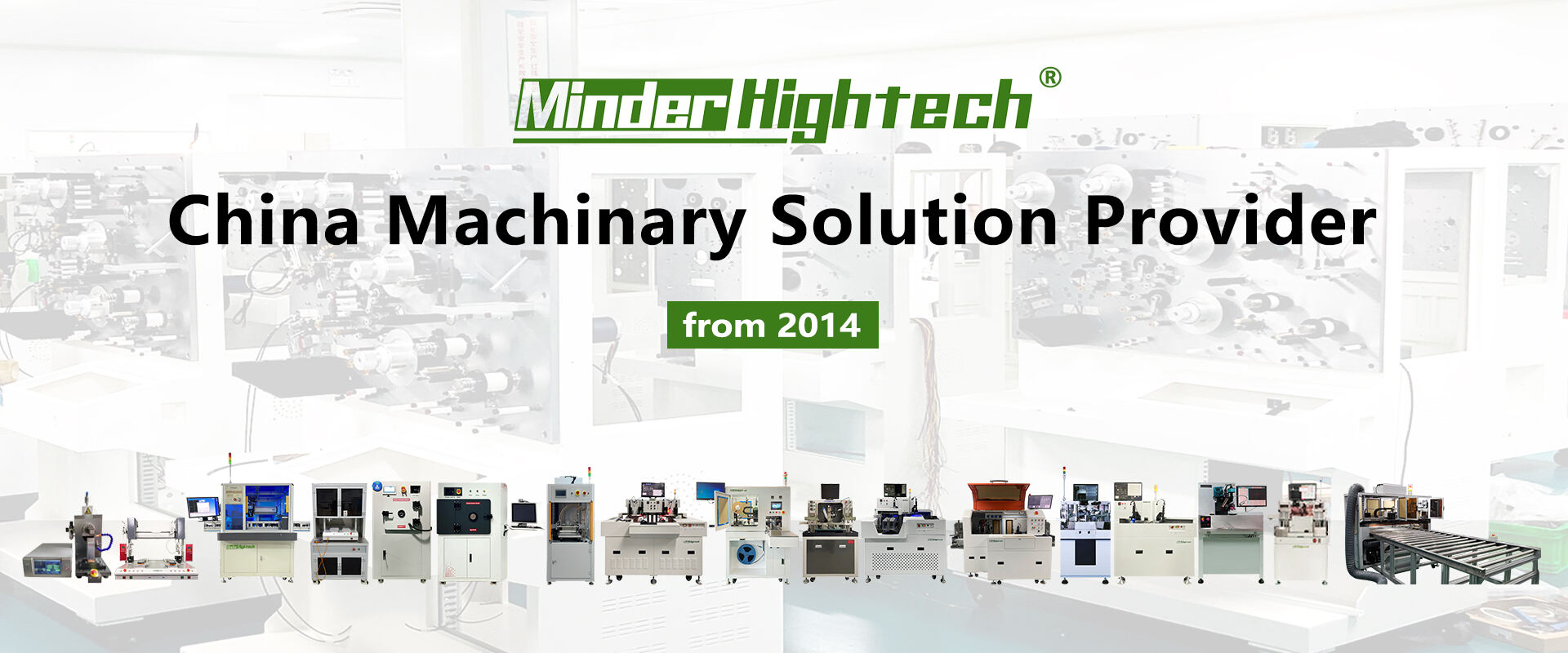
The machine first places the carrier, solder pad, and chip on the pulse heating table in sequence, and uses vacuum suction holes or fixtures to fix the carrier. When the carrier is placed on the hot stage, nitrogen gas begins to be released around the hot stage. When the chip is placed on the solder pad, the hot stage begins to heat according to the set temperature curve. After the solder melts, the suction head scrapes the chip to fully wet the solder. The parameters such as scraping frequency, path, amplitude, pressure, etc. can be set. After the cooling solder solidifies, the machine automatically puts the sintered chips back into the waffle box.
For experimental materials, different sizes of gold tin solder were mechanically cut using a cutting machine, followed by alcohol ultrasonic cleaning.
The carrier adopts a 1:2:1 Cu/Mo/Cu form, with Ni, Pd, and Au sputtered on the surface. Before application, it undergoes alcohol ultrasonic drying ultraviolet cleaning plasma cleaning process for backup use.
The chip adopts GaAs power chip. After the experimental materials are prepared, they are placed in the form of a waffle box on the feeding platform of the surface mount machine. Then, the temperature curve, pressure, scratching and other parameters are controlled through programming. The entire eutectic process is automatically completed by the surface mount machine, reducing the influence of human factors. Measure the shear force after eutectic completion.
Experimental results:
Eutectic temperature curve setting:
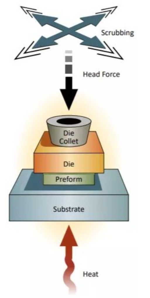
The eutectic temperature curve mainly includes three stages: preheating stage, eutectic stage, and cooling stage. The main function of the preheating stage is to remove water vapor inside the device and reduce thermal mismatch stress; The eutectic stage is mainly responsible for the formation of the eutectic layer molten alloy and is the most important stage in the eutectic welding process; The cooling stage is the process of cooling the device after eutectic completion, and the cooling temperature and rate will affect the magnitude of residual stress inside the device. The typical temperature curve is shown in Figure 1.
T2 is 30-60 degrees lower, T2 is the eutectic temperature, T3 is the cooling temperature, which can be set to 200-260 degrees. Due to the significant impact of eutectic temperature T2 on the quality of the eutectic layer, a single factor comparative experiment was conducted to determine T2. The analysis of the experimental results shows that when the hot table temperature is 320 degrees, the solder is completely melted and eutectic welding can be carried out. In order to increase the wettability and fluidity of the gold tin solder, the eutectic temperature is set to 320-330 degrees during gold tin eutectic welding.
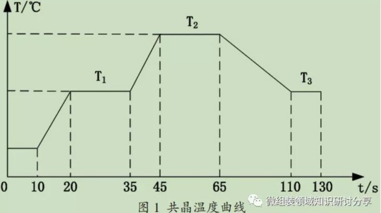
In addition, for the holding time of eutectic temperature T2, comparative experiments were conducted using scanning electron microscopy to observe the microstructure of the eutectic layer at different T2 times. The experimental results are shown in Figure 2.
Through comparative analysis, it was found that with the increase of eutectic time, the thickness of the IMC layer gradually increased from 0.373um to 1.370um, and the growth of IMC thickness slowed down after 160 seconds of eutectic. According to energy spectrum analysis, an IMC composite layer composed of (Au, Ni) Sn and (Ni, Au) 3Sn2 is formed at the solder/nickel interface. Analysis shows that during the eutectic process, the alloy Ni element gradually diffuses into the Au Sn alloy layer, causing the (Au, Ni) Sn layer with a small amount of Ni solid solution in the alloy structure to gradually increase, leading to the growth of the IMC layer.
The connection of heterogeneous metals in eutectic welding requires IMC, so a certain thickness of IMC layer can help improve the welding quality. However, the IMC layer is a brittle compound, and an excessively thick IMC layer can significantly reduce the shear strength of the weld. To ensure the formation of an appropriate thickness of IMC layer, the overall eutectic time is controlled at 2-3 minutes, with eutectic melting time of 15-30 seconds. Under these conditions, the thickness of IMC layer can be controlled between 0.3-0.9um, and the shear strength of eutectic chip exceeds 9.15Kgf.
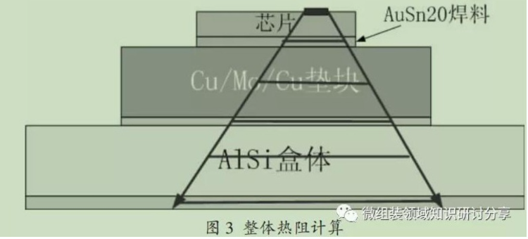
The advantage of eutectic welding over epoxy bonding lies in its lower thermal resistance, which can meet the heat dissipation requirements of high-power chips. Therefore, the thermal resistance of eutectic welding is very important. The thermal resistance of eutectic solder structures can be analyzed using the thermal resistance formula: R=h/K.S, where R is the thermal resistance value, h is the thickness of the solder layer, K is the thermal conductivity of AuSn20 solder, and S is the cross-sectional area of the solder;
For the overall structural thermal resistance, the model is shown in Figure 3. The analysis process is calculated based on the diffusion heat transfer in the active area, according to a 45 degree diffusion plan, and the cross-sectional area is calculated based on the effective area, that is, the length width product plan of the middle section of the trapezoidal surface.
Disclaimer: The content of this article is sourced from Micro Assembly (a knowledge seminar and sharing in the field of micro assembly). The copyright of the text, materials, images, and other content belongs to the original author. The content reproduced on this website is for everyone to share and learn from. If the legitimate rights and interests of the original author are infringed upon, please inform us promptly and we will arrange for the deletion of the relevant content.
Guangzhou Minder-Hightech Co.,Ltd.
Copyright © Guangzhou Minder-Hightech Co.,Ltd. All Rights Reserved
 EN
EN
 AR
AR
 BG
BG
 CS
CS
 DA
DA
 NL
NL
 FI
FI
 FR
FR
 DE
DE
 EL
EL
 IT
IT
 KO
KO
 NO
NO
 PL
PL
 PT
PT
 RO
RO
 RU
RU
 ES
ES
 SV
SV
 TL
TL
 IW
IW
 ID
ID
 LT
LT
 SR
SR
 SL
SL
 UK
UK
 VI
VI
 ET
ET
 HU
HU
 TH
TH
 TR
TR
 FA
FA
 AF
AF
 MS
MS
 GA
GA
 IS
IS
 HY
HY
 AZ
AZ
 KA
KA


