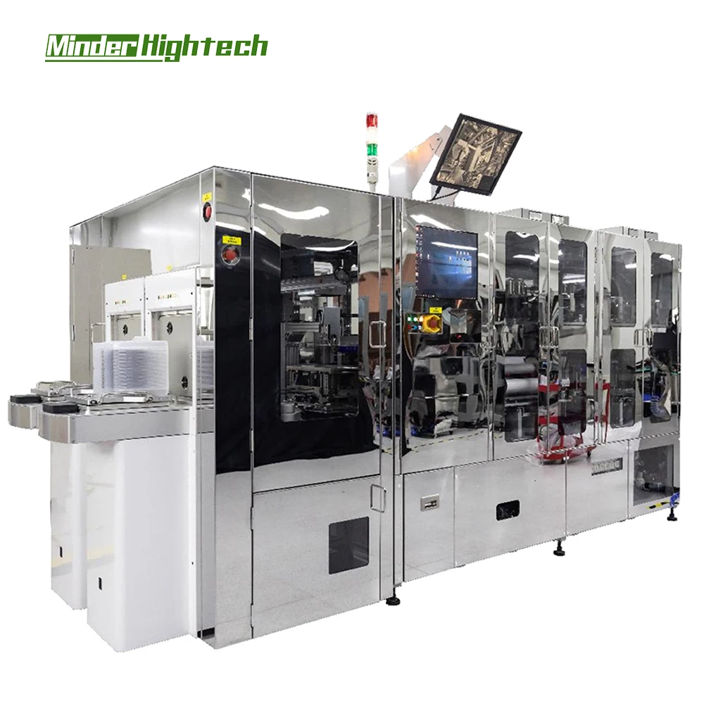
Wafer etching is a major process which involved in making electronics equipment that we are using on daily routine basis. The danger that Reactive ion etching poses to the production of microchips is something Minder-Hightech, a manufacturer of small electronic components, knows about first-hand. Step 1: Etching waferEtching the layer away from a flat piece that we call wafer, using a special approach. This is what moulds the wafer so that it can support small parts within microchips, and keep them properly.
In the present era, we have electronic equipment at every corner such as smartphones, tablets or computers. We depend on them for talking, viewing the monitor and even ready expert entails. All these devices require microchips to operate then Wafer saw hem in creating this microchip functioning. These helps make important microchip components such as resistors, transistors and other small parts. Without wafer etching, most of the electronics we are able to enjoy and use every day would not exist!
Wafer etching is a process used to do so, and there are various methods for Wafer dicing. The two generalized types of wafter construction techniques used in the manufacturing flow are wet etching or dry (plasma) based (= Reactive ion / photoresist strip). Wet etching — The wafer during wet etch processing is dipped into a special liquid solution to remove layers of the chip. This method is analogous to the idea of washing a wafer that has your unwanted parts. In contrast, dry etching works somewhat differently. It will be using ions or plasma to take away layers from the wafer without a liquid move. For each method, there are various pros and cons with the animation,time complexity itself all varies from one to another based on final output we want it to be seen or work as.
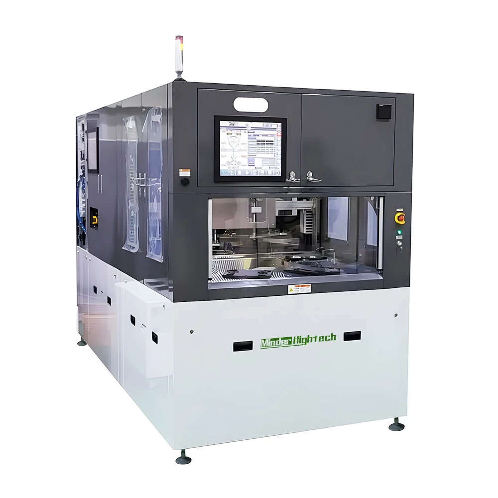
The demand for more sophisticated wafer etching technology is rising as people desire electronic devices. A deeper method is known as deep reactive ion etching (DRIE). With this technique, manufacturers can form three-dimensional (3D) features on the wafer enabling more design flexibilities. A third technique is more interesting since it makes use of lasers to carve the wafer. With lasers, the manufacturers can exert an almost equally precise control over how and where they remove material. Such precision is needed for manufacturing the high-quality microchips used in modern technology.
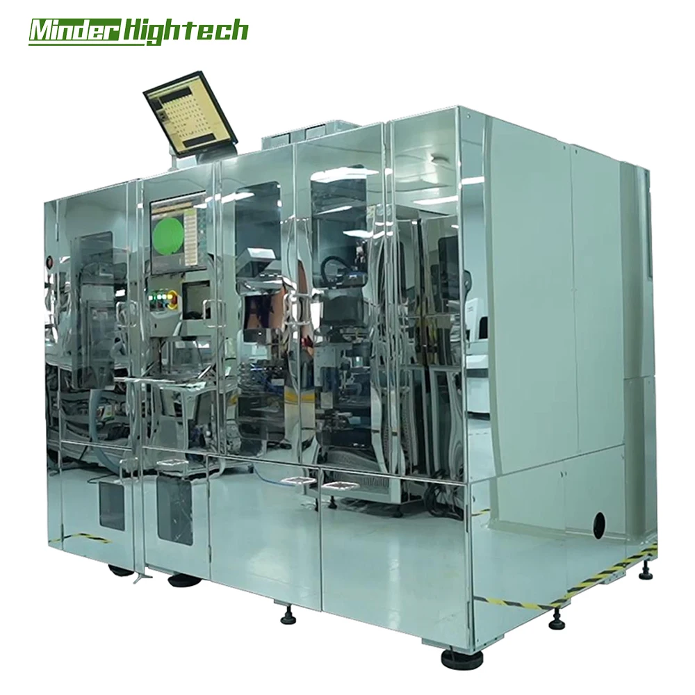
Chip etching in fact may have many challenges as any manufacturing process does. A common issue which can creep up is non-uniformity — the fact that layers are not fully stripped across the wafer. Imperfect purging like that can create defective microchips that are malfunctioning. One solution to this challenge is the use of plasma etching by manufacturers, which seeks to achieve even removal with techniques that are not purely mechanical. Contamination is another issue where dust or other small particles ends up on the wafer during etching. Wafer etching usually occurs in a clean space known as a cleanroom, to prevent contamination. They are engineered to be clean rooms, which means they are kept free from dirt and dust so that the wafers remain contamination-free until it is time for them to etch.
The microelectronics industry has experienced an impressive rate of growth in the last few decades and wafer etching is at center stage. Increase in usage of electronic devices is propelling the demand for better and accurate wafer etching techniques. Patents are improving and new methods keep the flow of innovative (and often micro-scale) approaches to enhancing the field; an effect mirrored in growth within both technology, business models all driving investment into enabling technologies which have contributed substantially to technical innovation deepening their roots behind much of industry progress. In order to satisfy this growing demand, companies like Minder-Hightech are continuously looking for ways to innovate in wafer etching and come up with new technologies.
wafer etching is comprised by a team of highly educated experts, highly skilled engineers and staff, who have exceptional professional experience and skills. The products of our brand are widely available in industrialized nations around the world, helping our customers to improve their efficiency, cut expenses and increase their product's quality.
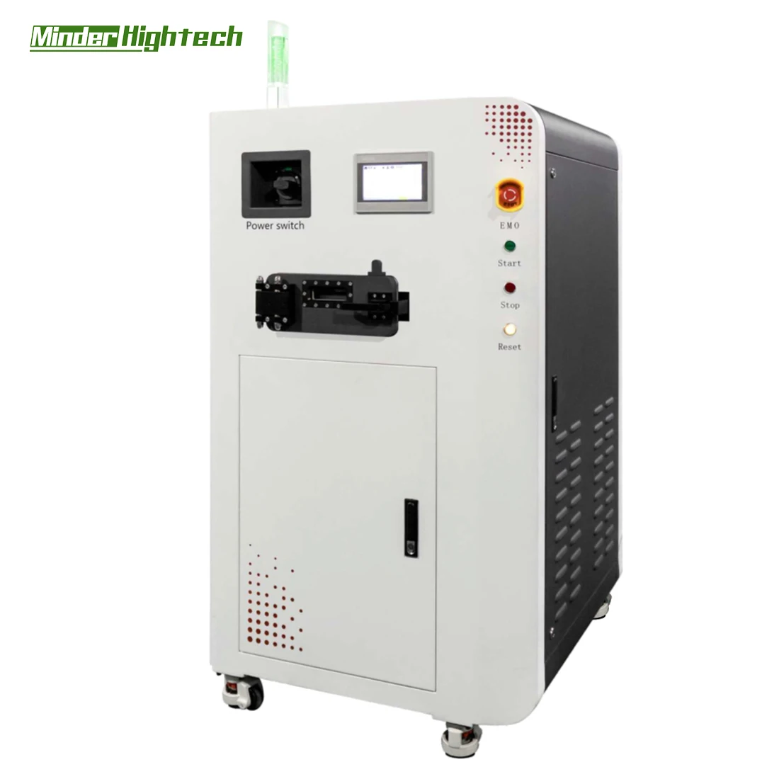
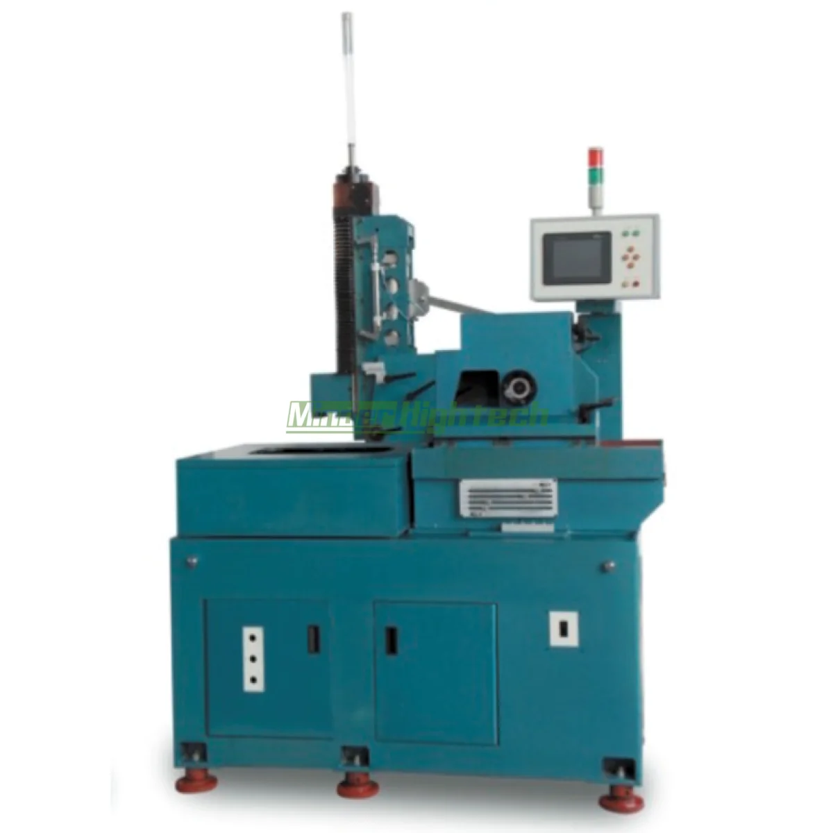
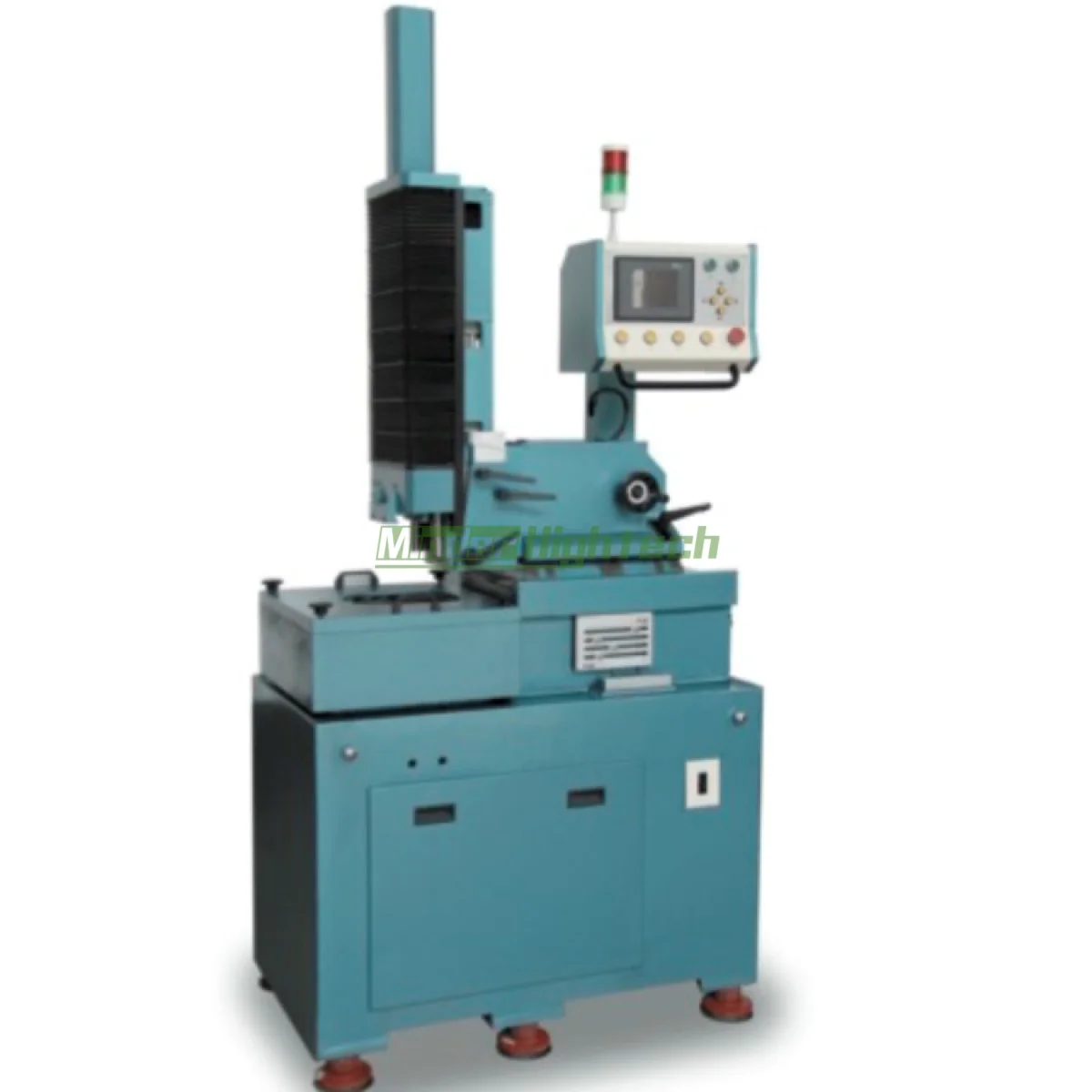
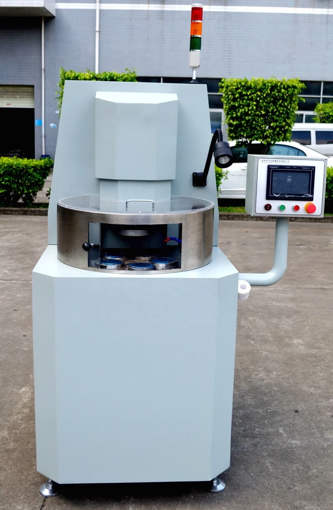
Minder-Hightech is a service and sales representative for electronic and wafer etching manufacturing equipment. Our experience with sales of equipment stretches over 16 years. The company is dedicated to providing its customers with Superior, Reliable, and One-Stop Solutions for machinery equipment.
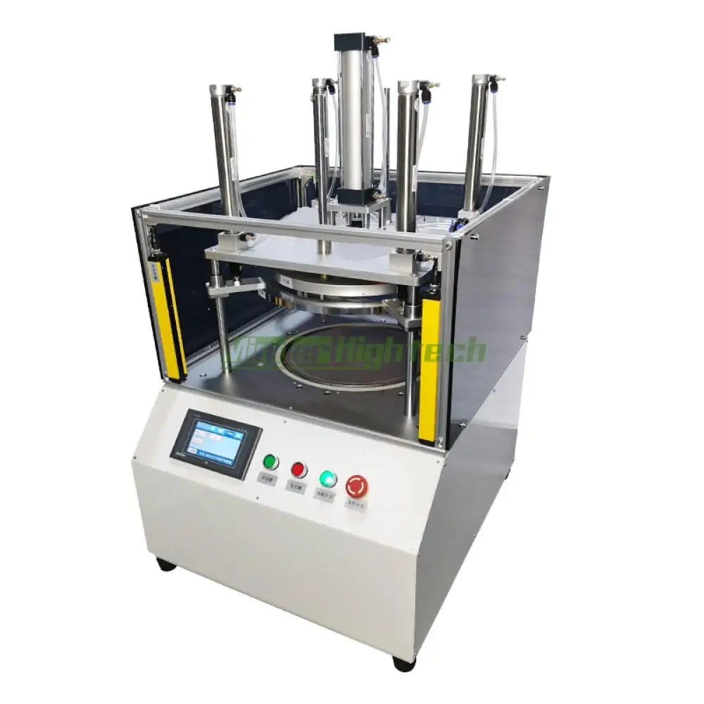
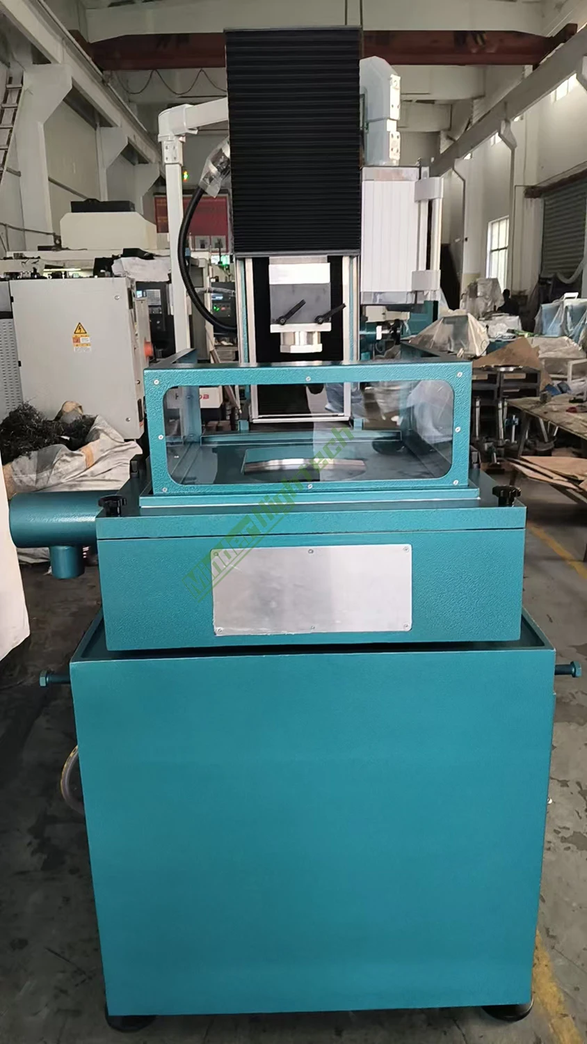
Our primary products are: wafer etching, Wire bonder Dicing Saw, Plasma surface treatment Photoresist removal machine Rapid Thermal Processing, RIE, PVD, CVD, ICP, EBEAM, Parallel sealing welder, Terminal insertion machine, Caparitar winding machines, Bonding tester, etc.
Minder-Hightech has become a popular brand in the world of industrial. With our many years of wafer etching in machine solutions and our long-standing relationships with overseas customers, we created "Minder-Pack" which focuses on the machine solution for packaging as well as other premium machines.
Guangzhou Minder-Hightech Co.,Ltd.
Copyright © Guangzhou Minder-Hightech Co.,Ltd. All Rights Reserved
 EN
EN
 AR
AR
 BG
BG
 CS
CS
 DA
DA
 NL
NL
 FI
FI
 FR
FR
 DE
DE
 EL
EL
 IT
IT
 KO
KO
 NO
NO
 PL
PL
 PT
PT
 RO
RO
 RU
RU
 ES
ES
 SV
SV
 TL
TL
 IW
IW
 ID
ID
 LT
LT
 SR
SR
 SL
SL
 UK
UK
 VI
VI
 ET
ET
 HU
HU
 TH
TH
 TR
TR
 FA
FA
 AF
AF
 MS
MS
 GA
GA
 IS
IS
 HY
HY
 AZ
AZ
 KA
KA