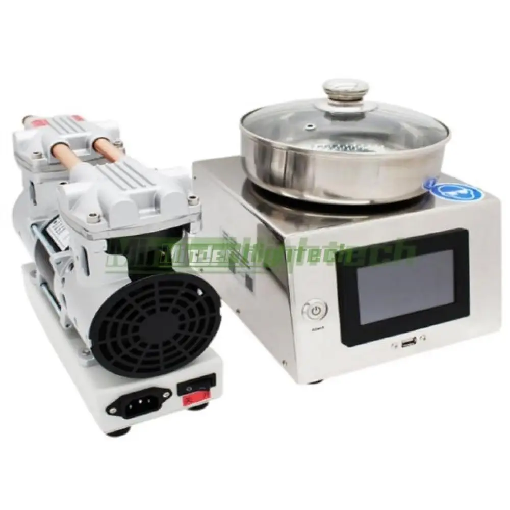
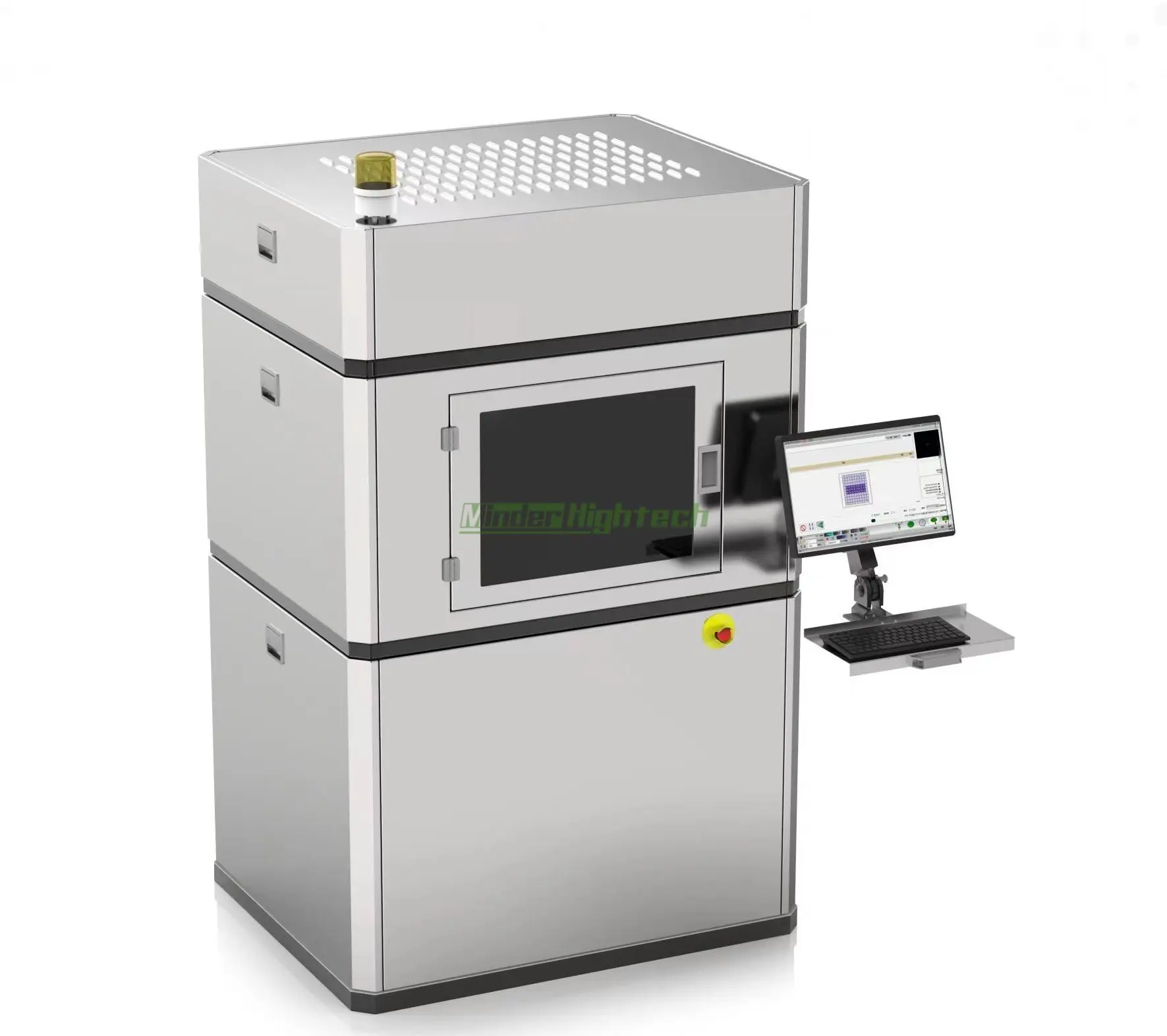
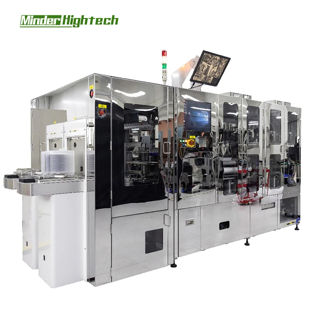
Have you ever heard of Wafer-Level Packaging Plasma Treatment? The term may sound a little buzz-wordy but its key for fabricating electronics in practical devices we use every day such as smartphones, tablets and computers. In this article, we will dig a bit deeper to understand what all needs to be done in order for it, why do you need that and how is it even helpful and helps us save further by reducing your chips land per square mm size as well helping the environment. Minder-Hightech Plasma surface treatment machine process or known as something else helps the electronic devices to perform better and durable. Plasma, a gas like substance gets driven into an enclosed chamber where tiny circuits (microchips) are present in this process. The plasma acts as a surfactant, removing contaminants such as dirt and dust from the surface of the microchips. This makes it easier for the microchips to work and eliminates situations where there would be issues further down the line.
During the production of electronics, something as small as a grain of sand or dust can lead to major issues. If there are any impurities during the manufacturing process, it can cause problems with how the device functions and make it break down earlier than intended. This is where the WLP Plasma Treatment would help. This Plasma Cleaning Machine process also increases the life of microchips by scrubbing them thoroughly, to erase any data leftover. This is particularly important for the devices that have to function in harsh circumstances, be it very low or high temperatures and pressures.
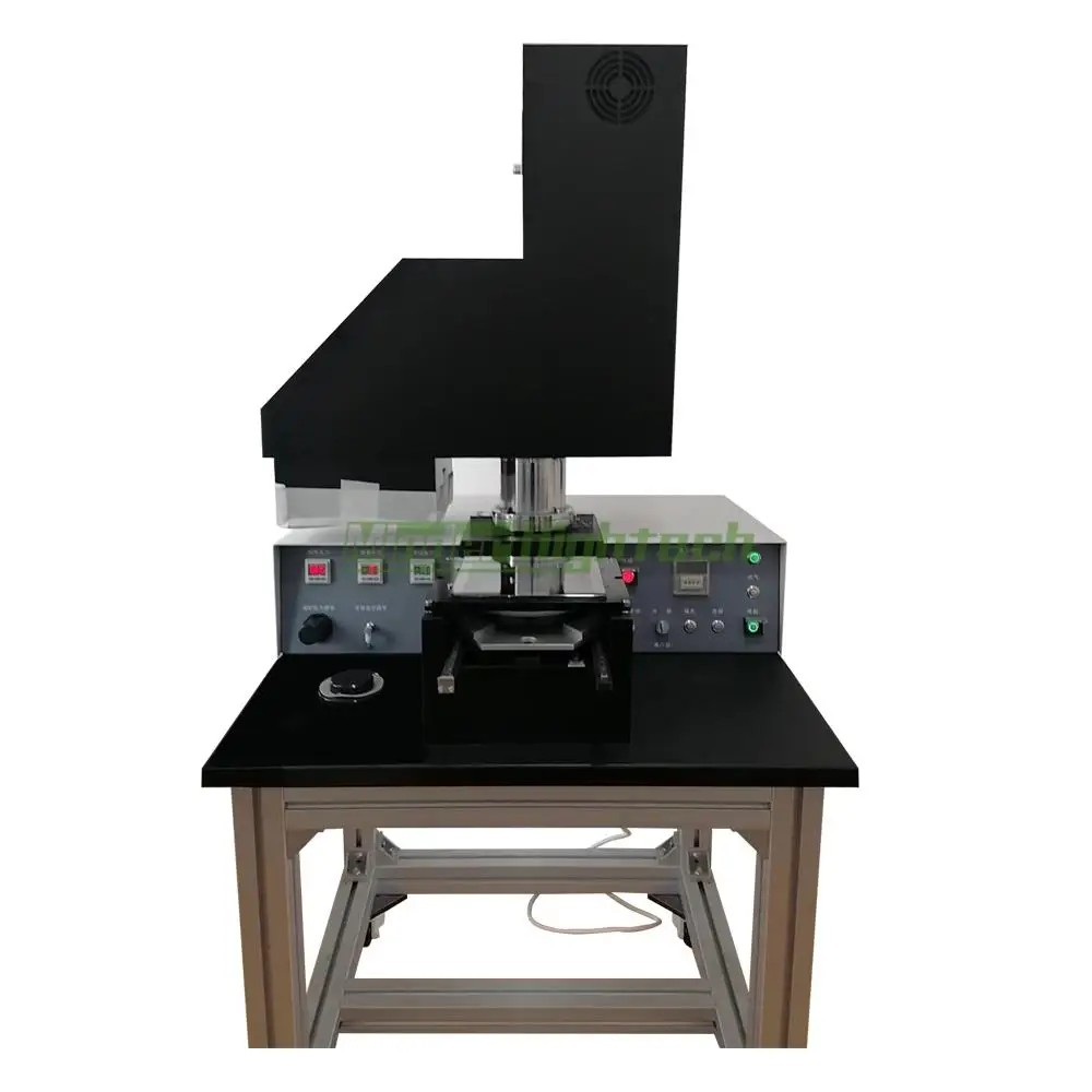
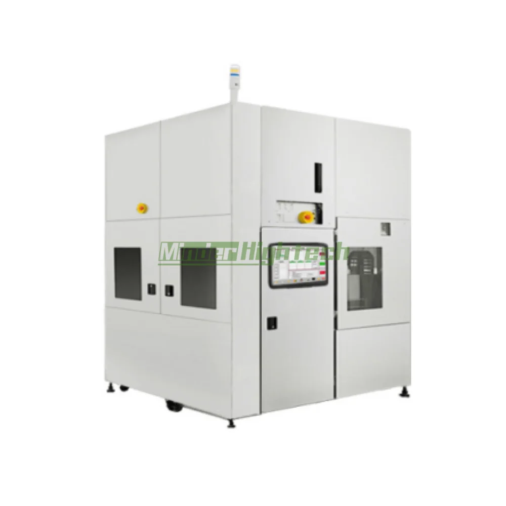
One of the significant issues they face in electronic world is how to make it smaller. We are packing more and more crucial components into a single microchip as technology advances, which is an incredible feat to achieve but it becomes even harder as the size of nano chips gets smaller. One important problem that is being troubleshooted with this Vacuum plasma surface treater. By removing the surface defects of microchip fabrication allows to accommodate more elements in a reduced area, with no side effects. What we can have is smaller, more powerful devices that are still lean and mean.
The more electronic devices we become dependent on, the greater our need for waste production in their manufacturing. Not only are these devices really easy to make, but it's also a super eco-friendly alternative—as making them the usual methods involve using chemicals that aren't great for our planet. Minder-Hightech Wafer cleaning solution is an even better answer, though. The process uses plasma, which is far safer than some of the harsh chemicals that were used previously. That makes less waste and ultimately a lighter footprint on the planet, which is good for every living being around.
Wafer-Level Packaging Plasma Treatment helps not only bettering the environment it saves manufacturers money as well. This step could be added to the existing processes which companies already use for manufacturing devices, without redesigning whole production lines. Manufacturers will save money repairing and replacing defective products by producing less waste and engineering more reliable devices. This Plasma Surface Treatment is good for both manufacturers and consumers: It keeps costs lower, which allows the manufacturers to sell better products at a low price point.
Minder Hightech is comprised by a group of highly educated experts, highly skilled engineers and Wafer-Level Packaging Plasma Treatment, with impressive professional skills and expertise. Since its inception, our products have been introduced to many industrialized countries around the world and have helped customers increase efficiency, cut costs and enhance the quality of their products.
Minder-Hightech has grown into a renowned brand in the world of Wafer-Level Packaging Plasma Treatment. With our decades of experience with machine solutions and our good relationships with overseas customers we developed "Minder-Pack" which focuses on the manufacturing solution for packages as well as other high-end machines.
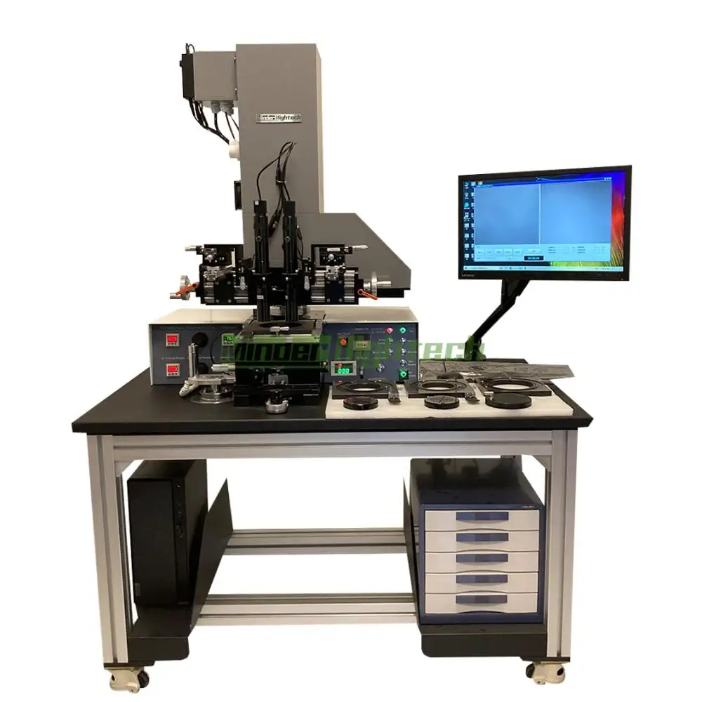
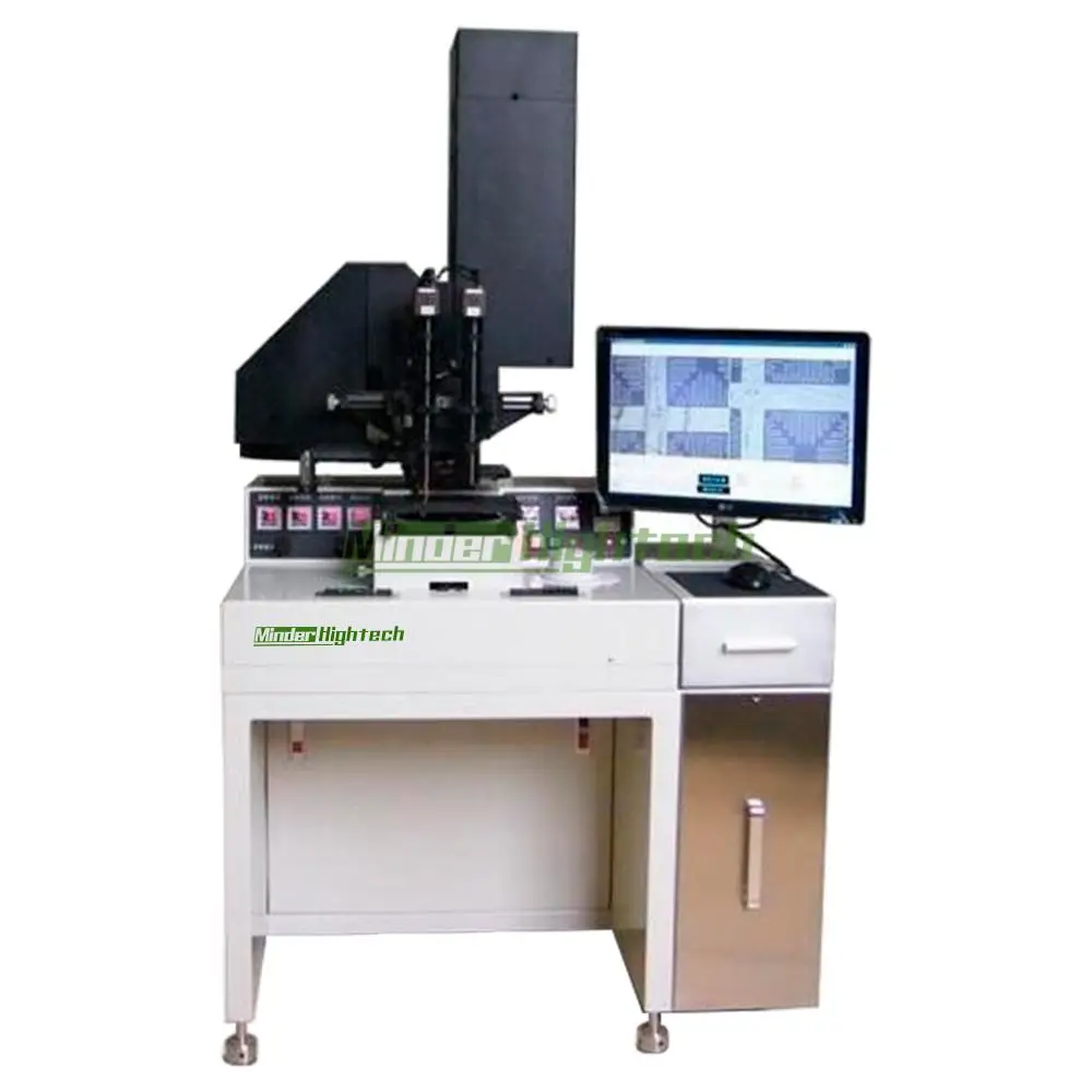
Minder-Hightech is a service and sales representative for semiconductor and electronic product industry equipment. We have more than 16 years of experience selling equipment. We are committed to offering customers Superior, Reliable and Wafer-Level Packaging Plasma Treatment for machinery equipment.
We provide a variety of products. Some examples Wafer-Level Packaging Plasma Treatment: Wire bonder and die bonder.
Guangzhou Minder-Hightech Co.,Ltd.
Copyright © Guangzhou Minder-Hightech Co.,Ltd. All Rights Reserved
 EN
EN
 AR
AR
 BG
BG
 CS
CS
 DA
DA
 NL
NL
 FI
FI
 FR
FR
 DE
DE
 EL
EL
 IT
IT
 KO
KO
 NO
NO
 PL
PL
 PT
PT
 RO
RO
 RU
RU
 ES
ES
 SV
SV
 TL
TL
 IW
IW
 ID
ID
 LT
LT
 SR
SR
 SL
SL
 UK
UK
 VI
VI
 ET
ET
 HU
HU
 TH
TH
 TR
TR
 FA
FA
 AF
AF
 MS
MS
 GA
GA
 IS
IS
 HY
HY
 AZ
AZ
 KA
KA