Creating microelectronics involves a lot of steps that should be carried out with caution. Wafer bonding is one such critical step. In reality, wafer bonding is putting two thinness materials or wafers as per their industry term together. It is important that whatever the two-points touch, hold a very strong adhesive property with one another for this process to work effectively. This is where surface activation comes in to play which aids bonding.
Surface activation of the wafer is a specific method applied to help increase adhesion or stickiness in wafer. Plasma treatment, UV/ozone treatment or chemical functionalization are some approaches that can be used to activate the surface. These techniques are different from each other and use to make wafer surface suitable for bonding.
It also serves to improve the quality of a microelectronic device. They help the wafers really all well together so that they reduce likelihood of problems like delamination. It will therefore perform better and last longer, hinting at increased robustness in whatever newfangled gadget it calls home.
Apart from enhancing the bond and quality of the device, surface activator also helps sprinkle wafer face with cleanliness. This way when you have an activation process done on the surface, any kind of dirt or contaminant which is not desirable can be taken out. This in turn should lead to a better, flatter surface from which they can print microelectronics on.
Finally, surface activation can make the wafer’s surface in a smooth nature. If we are using glue to stick two surfaces together then if the surface is too rough or bumpy it could be difficult for them to bond properly. A polishing or activation process can be performed to minimize roughness on the wafer surface that improves bonding and connection strength.
There are several concepts to consider when it comes to the science of wafer surface activation techniques. And one of these concepts is Surface Energy. For reference, Surface energy: the amount of energy used to produce a new surface. When two surfaces meet they bind according to their surface energy.
These surface activation techniques essentially provide some energy to the wafer, by increasing its surface energy. Such makes it easier for the wafer to stick onto another surface firmly, Methods in such as plasma treatment, UV/ozone treatment and chemical functionalization all generate active sites to a different degree increasing the surface energy of the wafer which is crucial for successful bonding.
Minder Hightech is comprised by a Wafer surface activation of high educated specialists, experienced engineers and staffs, with impressive professional skills and expertise. Until today, our brand's products have travelled to major industrialized countries around the world and have helped customers increase efficiency, decrease costs, and increase the quality of their products.
Minder-Hightech is now a very Wafer surface activation brand in the industrial world, based on many years of experience in machine solutions and good relationship with oversea customers of Minder-Hightech, we created "Minder-Pack" which focuses on the machinery on packages solution as well as other high-value machines.
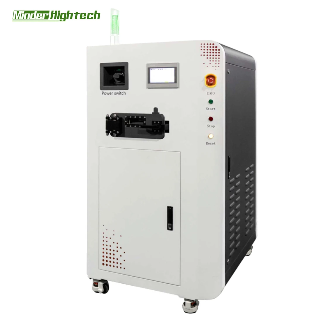
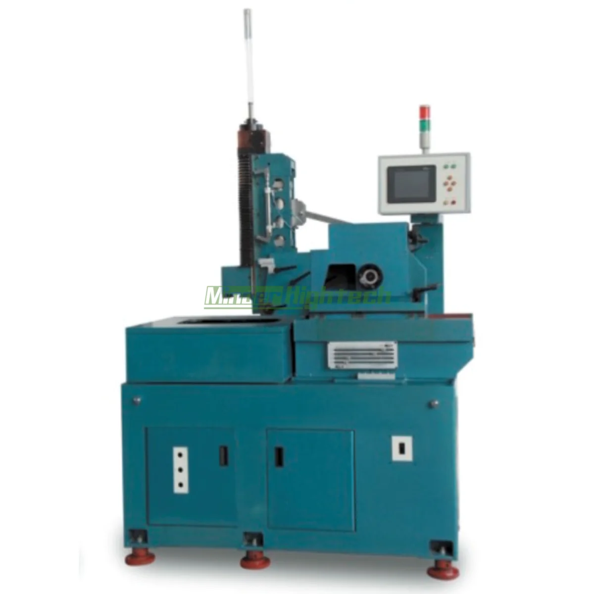
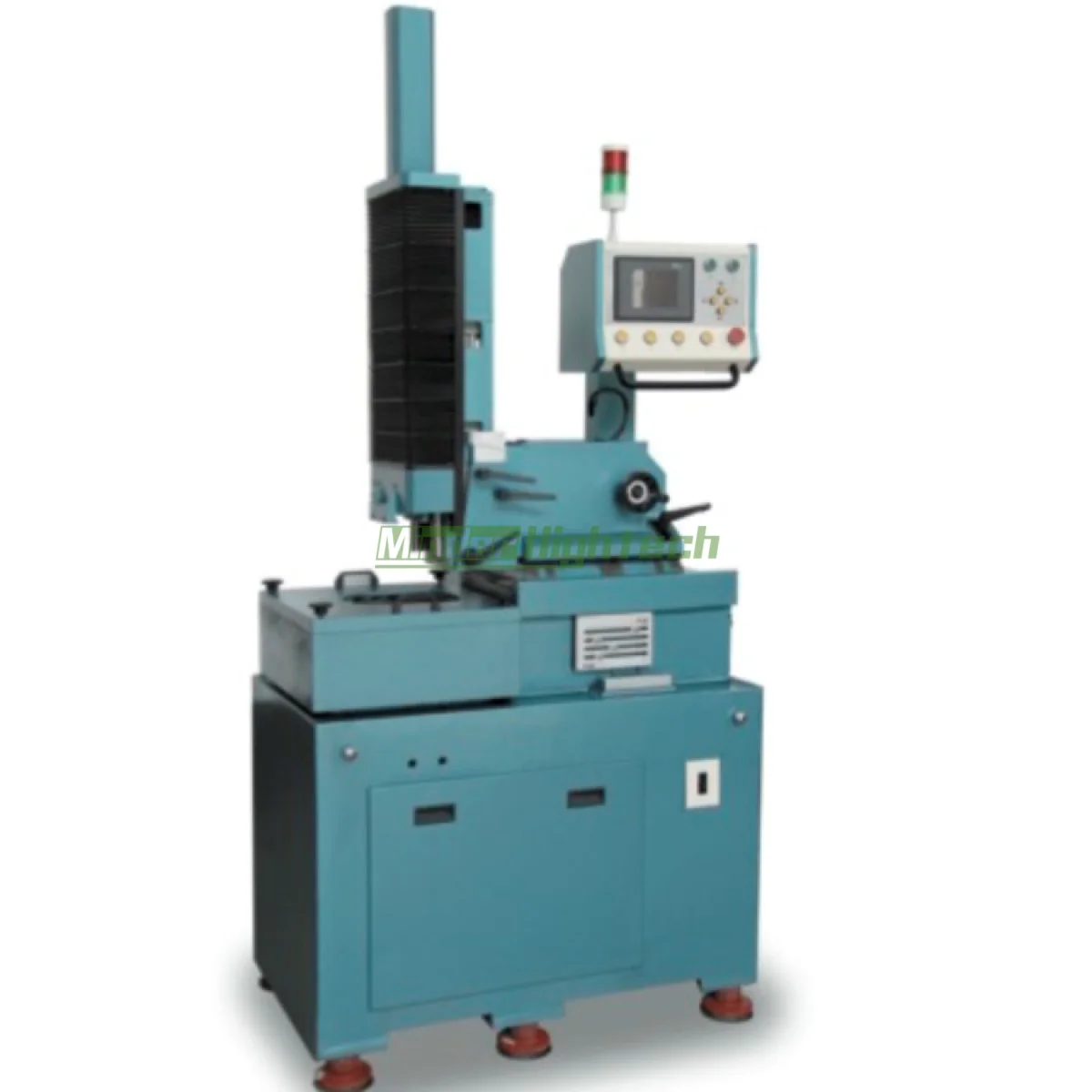
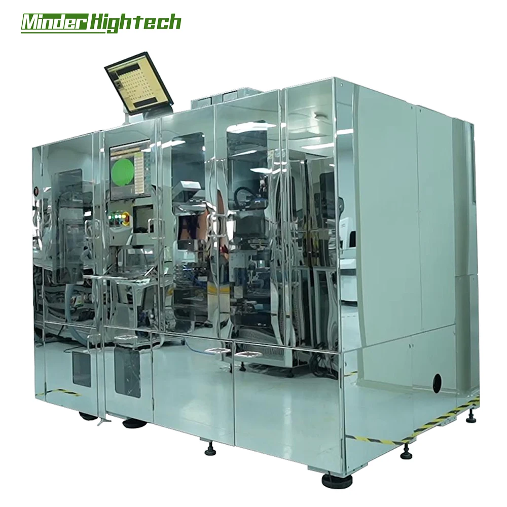
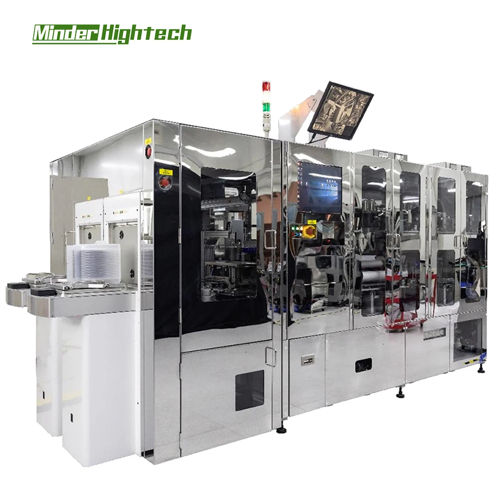
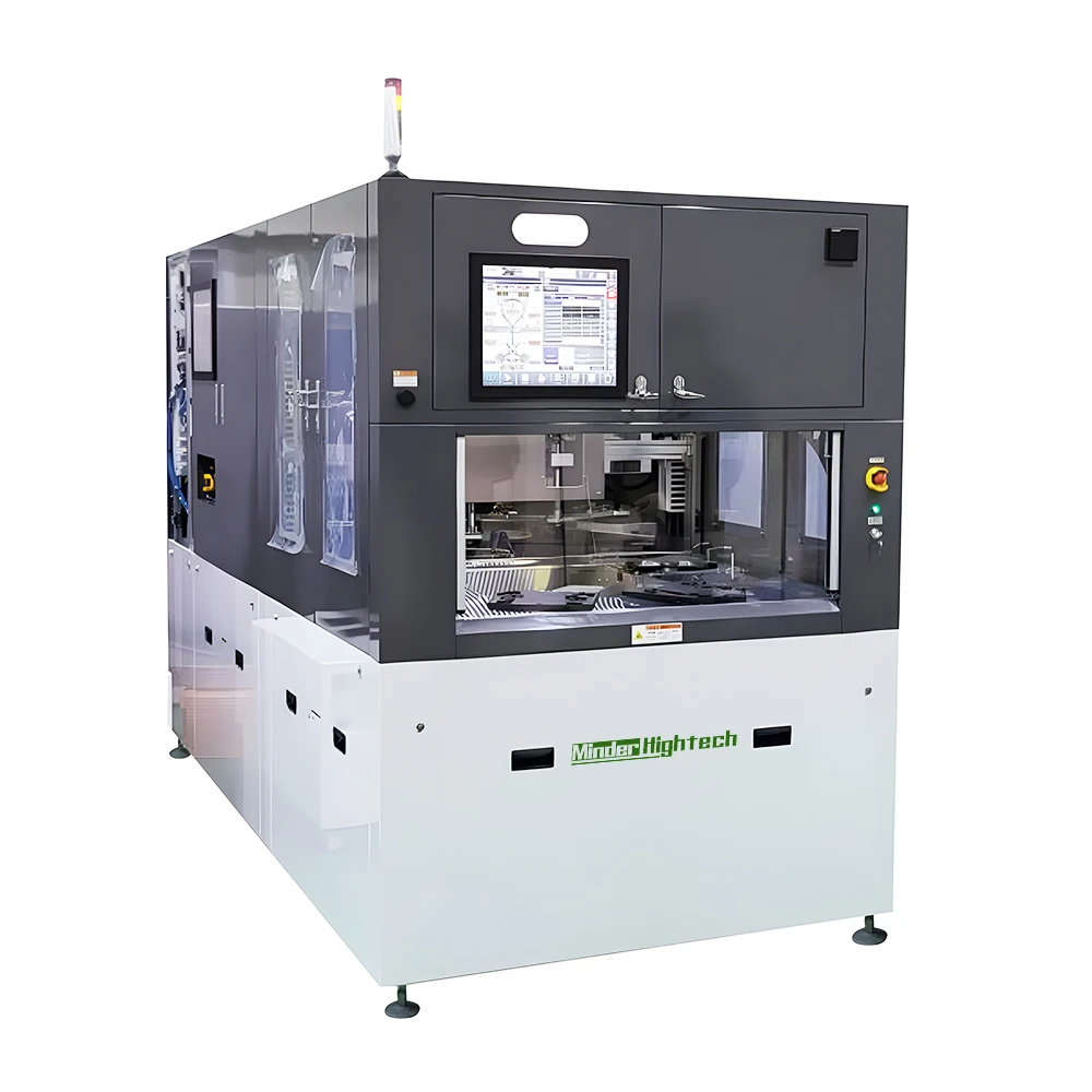
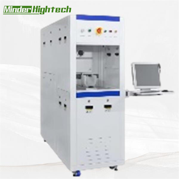
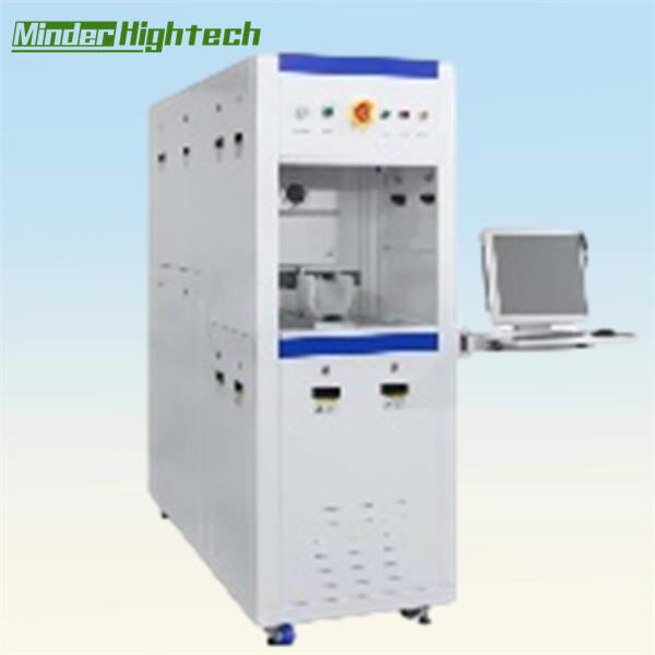
Our Wafer surface activation products are Wire bonder Dicing Saw, Plasma surface treatment Photoresist removal machine Rapid Thermal Processing, RIE, PVD, CVD, ICP, EBEAM, Parallel sealing welder, Terminal insertion machine, Caparitar winding machines, Bonding tester, etc.
Minder-Hightech Wafer surface activation the semiconductor and electronic products sector in service and sales. We have 16 years of experience selling equipment. The company is committed to offering customers Superior, Reliable, and One-Stop Solutions for machinery equipment.
Guangzhou Minder-Hightech Co.,Ltd.
Copyright © Guangzhou Minder-Hightech Co.,Ltd. All Rights Reserved
 EN
EN
 AR
AR
 BG
BG
 CS
CS
 DA
DA
 NL
NL
 FI
FI
 FR
FR
 DE
DE
 EL
EL
 IT
IT
 KO
KO
 NO
NO
 PL
PL
 PT
PT
 RO
RO
 RU
RU
 ES
ES
 SV
SV
 TL
TL
 IW
IW
 ID
ID
 LT
LT
 SR
SR
 SL
SL
 UK
UK
 VI
VI
 ET
ET
 HU
HU
 TH
TH
 TR
TR
 FA
FA
 AF
AF
 MS
MS
 GA
GA
 IS
IS
 HY
HY
 AZ
AZ
 KA
KA