Learning the fundamentals of chemical mechanical planarization in the semiconductor industry can be an exciting subject for students. Suppose we are in a world in which there are extremely accurate, advanced methods of making very small electronic things (eg using chemical mechanical planarization).
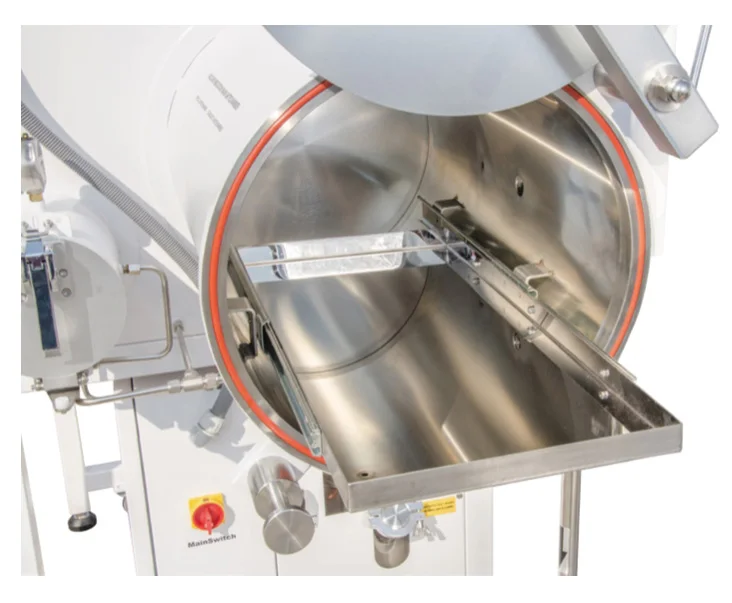
CMP, or Minder-Hightech Semiconductor Wire Bonding and chemical mechanical planarization, in short, is a technique employed in semiconductor fabrication to achieve a flat and smooth surface on silicon wafer. This is accomplished by a series of chemical and mechanical polishing processes, which remove irregularities and generate a smooth surface on which subsequent metal layer fabrication processes can be performed.
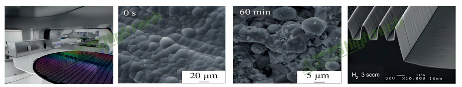
Obtaining a very flat plane in Minder-Hightech chemical mechanical planarization (CMP) is a requirement for the performance of semiconductor devices. “The vessel is only as stable as its base,” Professor Parson said in explaining how the sea ice influences the planet. At the same time in the Semiconductor equipment world, the flat surface is important to ensure equipment operates at its best performance.
The key to achieving high-performance semiconductor devices is excess material removal and minimizing perfect surface. Such can result in enhanced electrical conductivity and increased reliability of the Semiconductor saw device. CMP allows manufacturers to produce top-quality chips that underpin our daily gadgets.
It is indispensable in semiconductor production. There would be no way to produce the complex patterns and multilayered structures required for modern semiconductor devices without this fundamental process. And you see as what, the sort of finishing touch. The Semiconductor industry ensures that the final product is of the industrially stiff quality that's demanded.
Strides toward chemical mechanical planarization for next generation semiconductor technology are constantly being developed to meet the increasing demand of higher speed, smaller, and more powerful electronic devices. Companies are leading the way in solutions and challenging the limits of what can be achieved in Semiconductor Packaging solution manufacturing.”
Minder Hightech is comprised by a Semicon Chemical mechanical planarization of high educated specialists, experienced engineers and staffs, with impressive professional skills and expertise. Until today, our brand's products have travelled to major industrialized countries around the world and have helped customers increase efficiency, decrease costs, and increase the quality of their products.
Minder-Hightech has been a sought-after name in the industrial world. With our years of experience in the field of machine solutions as well as our excellent relationships with Semicon Chemical mechanical planarization we developed "Minder-Pack" that focuses on the machine solution for packaging and other valuable machines.
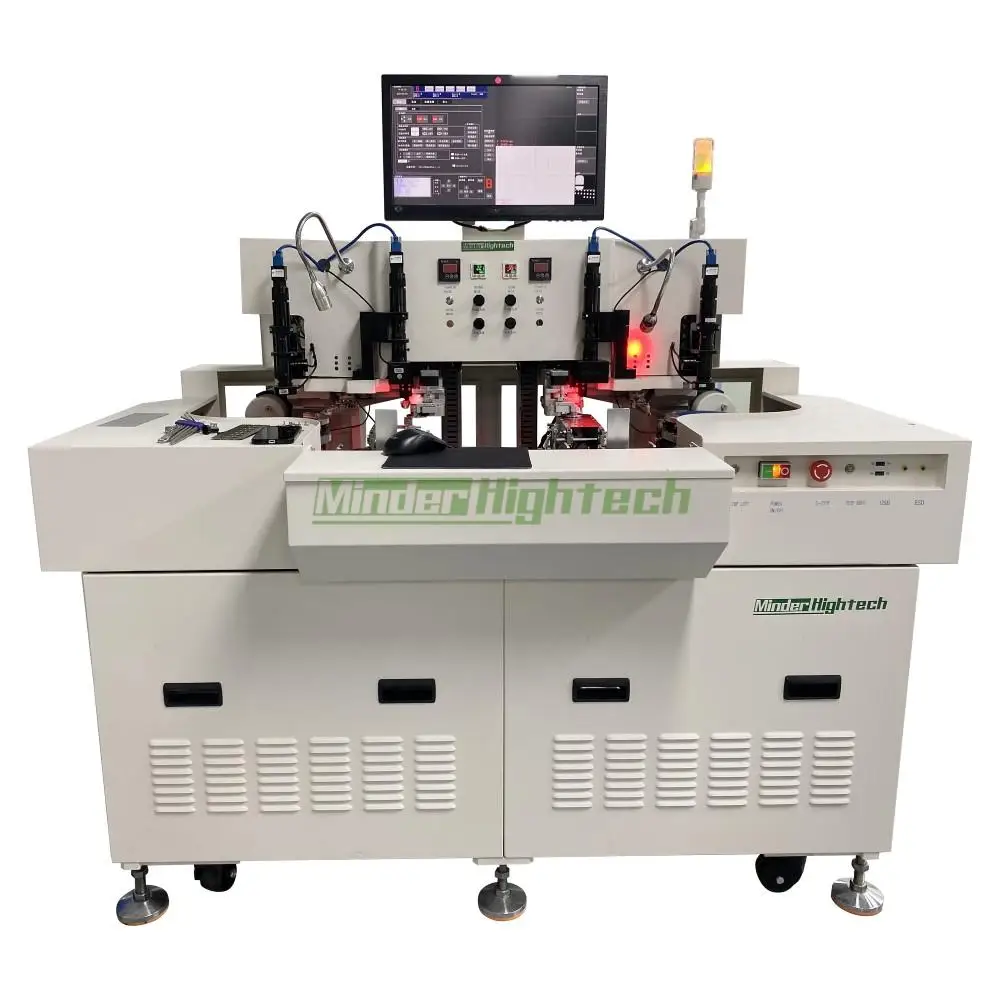
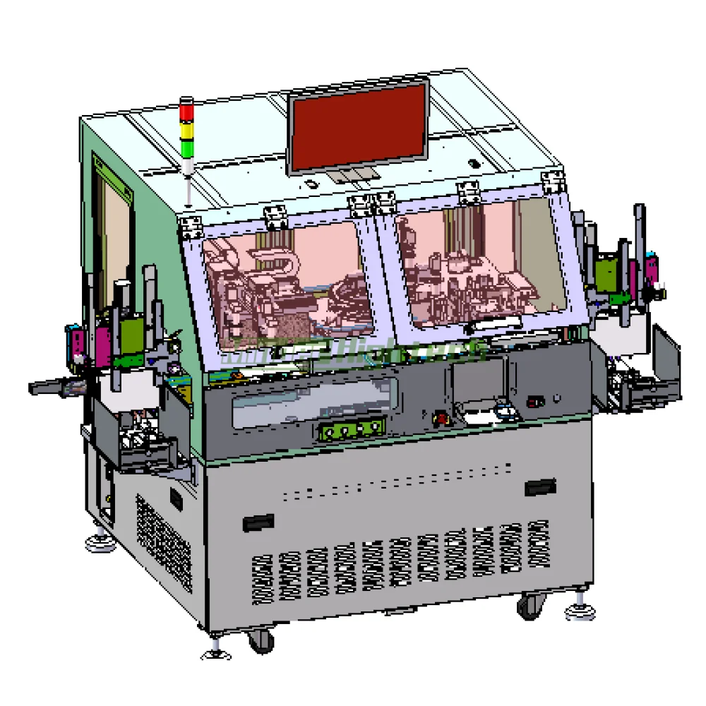
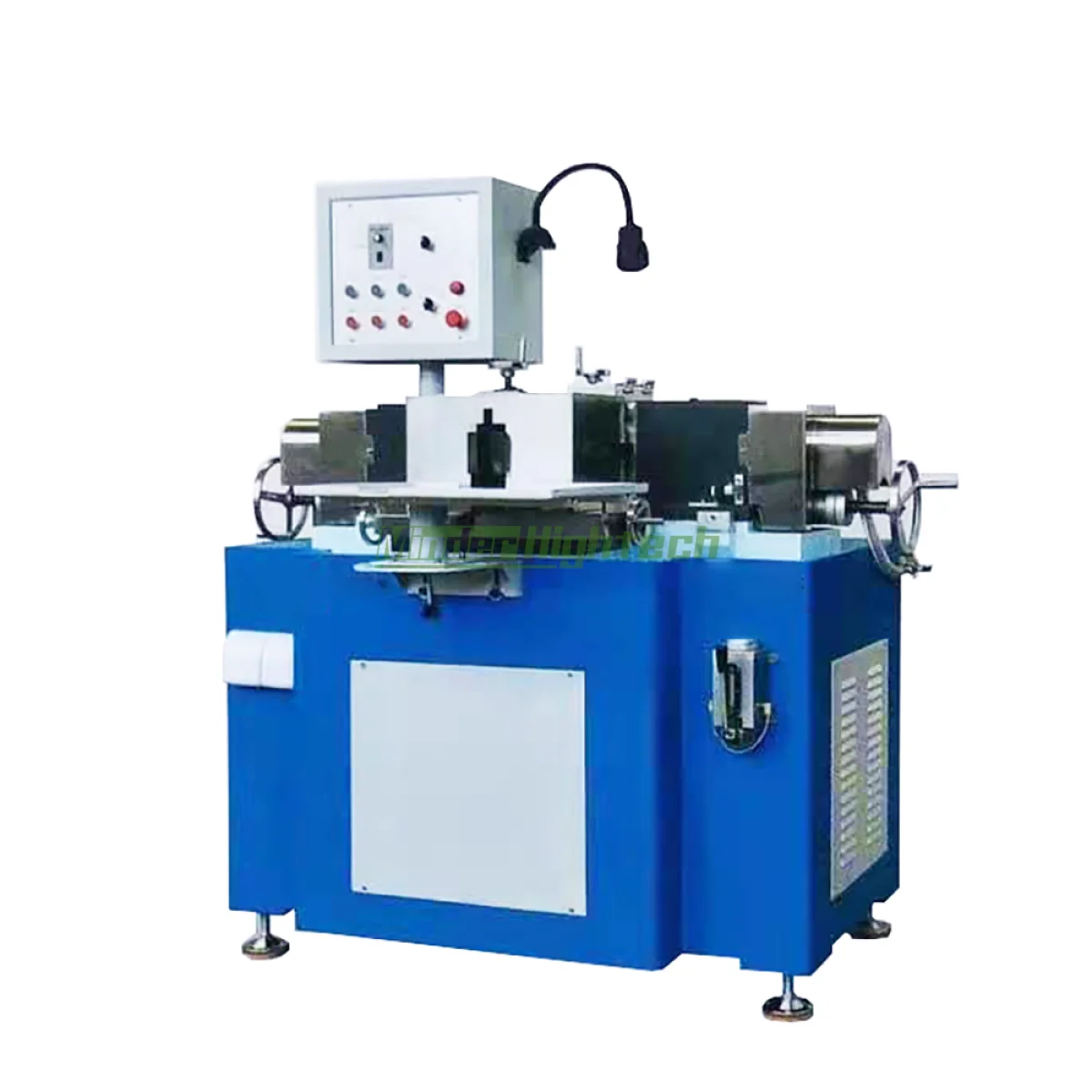
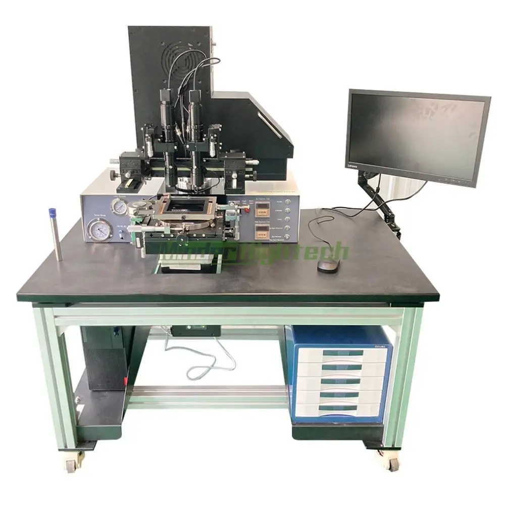
Minder-Hightech is a service and sales representative for semiconductor and electronic product industry equipment. Semicon Chemical mechanical planarization over 16 years of experience in sales and service for equipment. The company is committed to providing customers with Superior, Reliable, and One-Stop Solutions for machinery equipment.
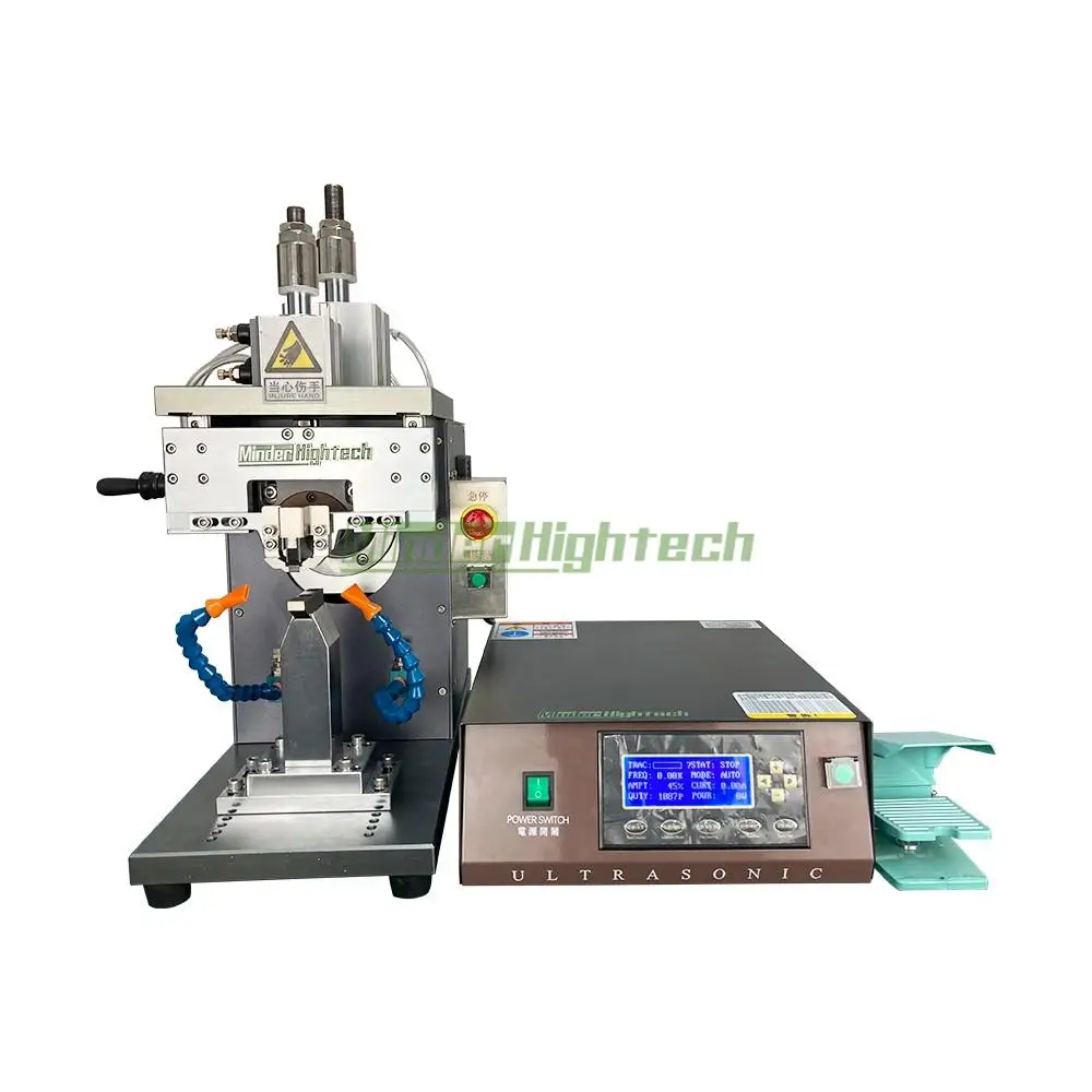
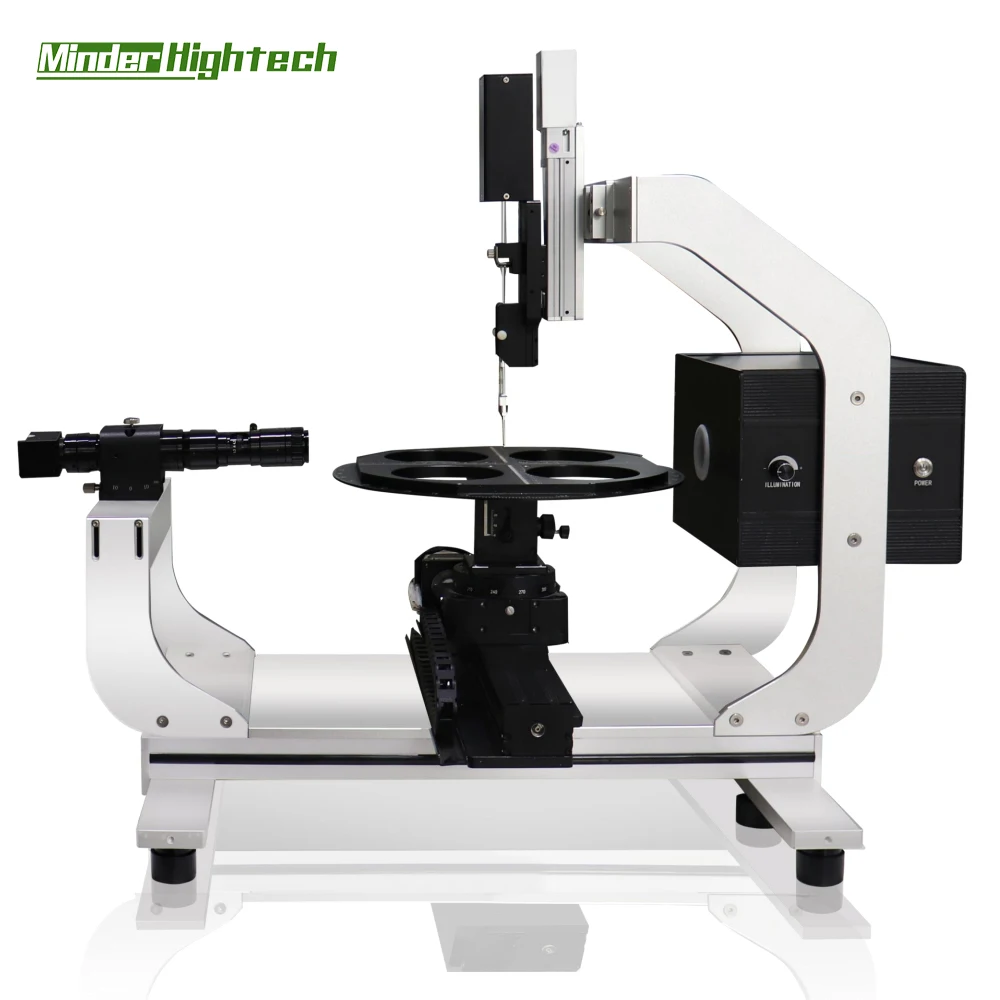
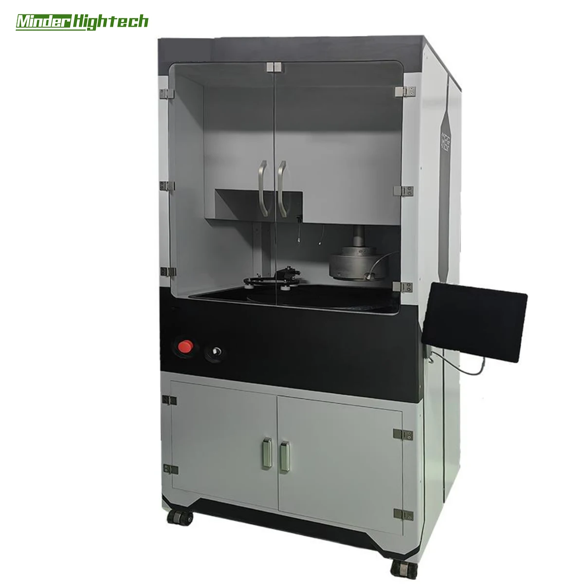
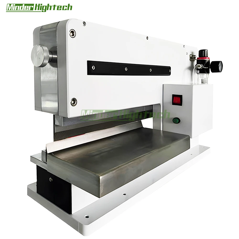
Our primary products are: Semicon Chemical mechanical planarization, Wire bonder Dicing Saw, Plasma surface treatment Photoresist removal machine Rapid Thermal Processing, RIE, PVD, CVD, ICP, EBEAM, Parallel sealing welder, Terminal insertion machine, Caparitar winding machines, Bonding tester, etc.
Guangzhou Minder-Hightech Co.,Ltd.
Copyright © Guangzhou Minder-Hightech Co.,Ltd. All Rights Reserved
 EN
EN
 AR
AR
 BG
BG
 CS
CS
 DA
DA
 NL
NL
 FI
FI
 FR
FR
 DE
DE
 EL
EL
 IT
IT
 KO
KO
 NO
NO
 PL
PL
 PT
PT
 RO
RO
 RU
RU
 ES
ES
 SV
SV
 TL
TL
 IW
IW
 ID
ID
 LT
LT
 SR
SR
 SL
SL
 UK
UK
 VI
VI
 ET
ET
 HU
HU
 TH
TH
 TR
TR
 FA
FA
 AF
AF
 MS
MS
 GA
GA
 IS
IS
 HY
HY
 AZ
AZ
 KA
KA