 EN
EN
 AR
AR
 BG
BG
 CS
CS
 DA
DA
 NL
NL
 FI
FI
 FR
FR
 DE
DE
 EL
EL
 IT
IT
 KO
KO
 NO
NO
 PL
PL
 PT
PT
 RO
RO
 RU
RU
 ES
ES
 SV
SV
 TL
TL
 IW
IW
 ID
ID
 LT
LT
 SR
SR
 SL
SL
 UK
UK
 VI
VI
 ET
ET
 HU
HU
 TH
TH
 TR
TR
 FA
FA
 AF
AF
 MS
MS
 GA
GA
 IS
IS
 HY
HY
 AZ
AZ
 KA
KA

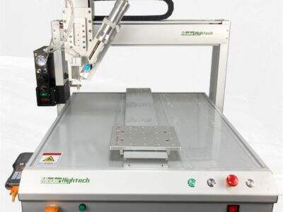
The Inductively Coupled Plasma (ICP) etching is a widely employed technique in several industrial sectors, such as VLSI fabrication. That is the technique we can use to etch patterns into materials such as silicon wafers. One typical wafer dimension is 4˝, and many companies need to understand ICP's ability to etch deep (in this case into a 4˝) into these wafers. Etching depth, at Minder-Hightech we are the best with all types of etching and know that understanding which one to use is important for our clients.
How Much Does Inductively Coupled Plasma Allow 4-Inch Wafers to be Acid Etched?
The maximum etching depth is not constant for 4-incb wafers since ICP is employed. In general, you are able to reach the depth of a few micrometers up to a few hundred micrometers, depending upon the exact technique used. For example, a typical target might be on the order of 100 micrometers deep, but with the right settings, some systems could go deeper. It is important to note that a deeper etching will need precise monitoring of the process parameters, such as gas flows rate, pressure and power. All of these factors contribute to how deep you’re able to etch.
If you raise power during etching, then you might get the higher etching rate. But the current will also tend to cancel itself out, you get -rough surfaces, since it's looking for protein. At Minder-Hightech, we will not compromise Speed of Etching with Quality. It’s a balance, and we design our systems around having the best of both worlds so that while you might screen a viable etch depth, you’re also keeping your wafer intact.
Clients frequently inquire as to how long they will need to etch something to a certain depth. For example, the etching rate may be within the range of 0.1 to 1 μm/min according to material and process conditions. Thus, more time is required for further etching. It seems a bit like digging a hole; the deeper you want to go, the more time and effort it will require. By knowing these factors our clients can be more informed when it comes to etching for their projects.
On the Tilted Sidewall in ICP Etching: What Determines the Slope of a Sidewall?
The slant of the sidewall 3a is another consideration of ICP etching. A steep sidewall is good in that the walls of the etched pattern are close to vertical which is desirable for many applications. The numbers for how steep the sidewalls can be are influenced by a few things. The chemistry of the etching gases is considered as one of the major reasons for that. Various gases interact differently, producing different sidewall angles.
For instance, the use of a fluorine containing gas mixture in addition to an argon gas can aid in providing steep side walls. The rates at which these gases flow are important too. If you have too much of one gas, it can lead to a side effect known as “micro-masking” that can reduce sidewalls’ steepness. At Minder-Hightech we optimize these gas mixtures and flow rates to help us achieve the desired sidewall angle for their specific requirements.
Another factor is the intensity of the plasma. More power can mean a more aggressive etch, which could aid in steepness but also bring unwanted roughness to the sidewalls. This has proved to be a tricky balance. The temperature of the wafer may also be a factor. If the wafer is too hot, you will get less steep walls.
Finally, the etching chamber pressure also can influence sidewall angle. Lower pressure typically leads to flimsier sidewalls while high inflation can produce a kind of roundness. These parameters must be tuned very carefully for the best results. By understanding these elements, as specialists in Minder-Hightech we can aid to the quality of etching that is most suited for our clients and we offer best performance especially when 4 inch silicon wafers comes into play.
What Is the Maximum Etch Depth on a CSD Etched by Various Plasma Sources?
Etching is a process which is heavily utilized in the field of electronic devices. It is useful for taking away particular areas of materials on a wafer, or thin slice, of semiconductor. The depth of the etch could be dependent on the kind of In-Line plasma technology applied. For instance, inductively coupled plasma (ICP) is an etching method, regarded as the most excellent. It is capable of deep etching depths, particularly for 4-inch industry standard wafers. ICP is based on RF energy generation of plasma. This plasma then collides with the material on the wafer and strips it, layer by layer. The etch depth can be considered as a function of several parameters, as the plasma power and the gas species. Typically, with ICP technology etch depths of a few micrometers can be obtained. This can be very handy for making small features required in modern electronics. In addition to ICP, other plasma techniques such as reactive ion etching (RIE), may be utilized if they access not a deeper depth than ICP. RIE sometimes lack depth but are very accurate and can be used for a variety of applications. At Minder-Hightech, our priority is to offer your business superior ICP systems capability that delivers the best etching depths for your 4-inch wafers and offers you the most efficient performance from your applications.
Where is the Place to Find Top Grade Inductively Coupled Plasma Systems that You Can Afford?
It can be difficult to find the best things for engraving, particularly if you're searching for a high-quality item at a good price. One option is to hunt for companies that specialize in Inductively Coupled Plasma systems, such as Minder-Hightech. They provide a range of ICP ranges to suit your requirements and budget. Amoung these, some of the Plasma cleaning systems, you should cogitate when looking for are as below: For example, consider the maximum etching depth you need and how quickly you would like it done. You can begin by going to the official website of the company, or would rather get in touch with their sales team and explore yourself on what they have in store. Plus, it's good to see the reviews and hear what other people in the industry are recommending. Occasionally, companies offer special deals or discounts as well, particularly if you buy more than one system. You can also check out trade shows or tech expos. Such events often attract companies to present their latest tech. That way, you can watch the systems in practice and put questions to the experts. Never forget to compare the item before a decision is made. And not to forget that high quality ICP systems from Minder-Hightech are best way of assuring that you etching is being done in a reasonable time and is usable.
How to optimize the etching efficiency of inductively coupled plasma on 4 inch wafers?
If you want your Inductively Coupled Plasma systems to perform at their best, you need to think in terms of efficiency. You can do a number of things to reach that point. First of all, ensure that you have the right settings for your specific materials. Other materials may require different gas mixtures, power levels, and pressure parameters. Spending time to fine tune these will provide you with a more ideal etching depth and quicker etch. The regular servicing of your ICP system is very important as well. This may include washing the parts and inspect them for wear. A regularly maintained Inductively coupled plasma will run so much better and even last longer. Another is to watch the process. Employ sensors and data collection aids to see how the etching is going. That way, you can identify problems early and adjust if necessary. It is necessary to train your team on the ICP system usage best practices. When everyone knows how to use the utensils, everyone gets better results. At Minder-Hightech, we also offer training and support to ensure you get the most out of your ICP systems. By baking these recommendations, we are confident that your etching procedures will be efficient and deliver high quality results for the 4” wafers.
Table of Contents
- How Much Does Inductively Coupled Plasma Allow 4-Inch Wafers to be Acid Etched?
- On the Tilted Sidewall in ICP Etching: What Determines the Slope of a Sidewall?
- What Is the Maximum Etch Depth on a CSD Etched by Various Plasma Sources?
- Where is the Place to Find Top Grade Inductively Coupled Plasma Systems that You Can Afford?
- How to optimize the etching efficiency of inductively coupled plasma on 4 inch wafers?


