The first thing we do is coat the surface of the base material with a special light-reactive material. It is photosensitive material, which has a key role in the process. Then we use a mask with some kind of pattern on its surface, and put it above that layer. The mask serves as a stencil with holes that transmit light through select locations. Next, we expose the pattern on the mask to UV light that we cannot see. This light creates an image of the photosensitive material, similar to how sunlight can create a shadow when you shine it through a cutout shape. The final step consists of us soaking the substrate in a type of solution known as a developer. This process eliminates the section of photosensitive layer exposed to light and presents a pattern on the base material.
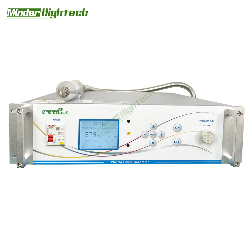
In Wire bonder one of the biggest parts that has to be controlled are the mistakes that occur during the three main steps and it is very important to get good, accurate results. Coating a) The coating involves covering the base material uniformly with the photosensitive material. That is, each piece of the base material has to have the same dose of special ingredient. In other words, we normally use machines to achieve that perfect straight and leveled surface. During this step, we verify the quality (no bumps or flaws surface side)
The developer solution is used to remove the exposed section of the material, creating a pattern during step 3; development. But we can still get this step wrong. We do not want to leave the material in the solution too long and if our solution is too strong, it will eat away at the pattern we are trying to create. So, we need to very carefully control the timing and concentration of the developer solution in order to get good results.
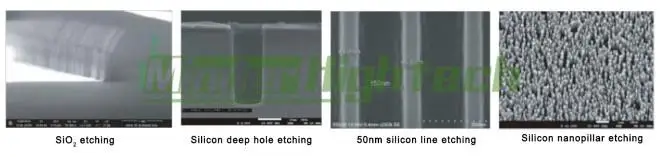
The primary benefit of Wire bonding machine is the capability to image extremely small components. This allows us to produce very small, high-performing parts. The method is also very advantageous for mass production; it permits us to manufacture many parts within a short period of time. This is particularly crucial in industries with an extremely high demand for a certain type of identical parts (like the electronics-making industry).
On the other hand, there are some cons as well. The high cost of mask aligner photolithography in terms of the machines as well as the materials used for it is one of the largest challenges that come with this method. The machines can be prohibitively expensive, and we require high quality raw materials for which too cost an arm and a leg Also, it is not possible to make features smaller than i.e. 10 nm with this type of method This is significant because we are so often pushing the building of ever smaller and more powerful things. In addition, the process is extremely prone to contamination so it must be performed in a very clean environment (usually called a cleanroom). The requirement for This can make Things a bit more complex and more expensive.
In areas from electronics to medicine, mask aligner photolithography is predicated on fundamental research and development. The application of SU-8 is absolutely essential in the electronics industry for manufacturing microelectronic devices such as integrated circuits, sensors and displays. The making of these structures has required numerous special tools built to perform this work, with good examples being the EVG(R) mask aligner and EVG(R) wafer bonding system.
For example, in medical research, photolithography is used to construct microscopic canals for the analysis of body fluids; this technology is part of what is called a lab-on-a-chip. Using this technology, fluids can be analyzed rapidly and with precision to shed more light on a patient's health. The use of a mask aligner in photolithography for fabricating micro and nanofluidic systems is also possible. If correct, these systems would increase the precision of drug dosages for patients, improving efficacy and safety of treatments.
Minder Hightech comprises a team of highly educated engineers, professionals, and staffs with outstanding expertise and experience. Our brand's products have spread to major industrialized countries across the globe aiding customers to improve efficiency, mask aligner photolithography and increase the quality of their products.
Minder-Hightech is sales and service representative of electronic and semiconductor products industry equipment. Our experience with sales of equipment stretches over 16 years. We're committed to providing customers Superior, mask aligner photolithography and One-Stop Solutions in the field of machine tools.
Minder-Hightech mask aligner photolithography become a well-known brand in industrial world, based on the years of machine solution experience and good relationship with oversea customers from Minder-Hightech. We created "Minder-Pack" which focuses on the manufacturing of packages solution, as well as other high value machines.
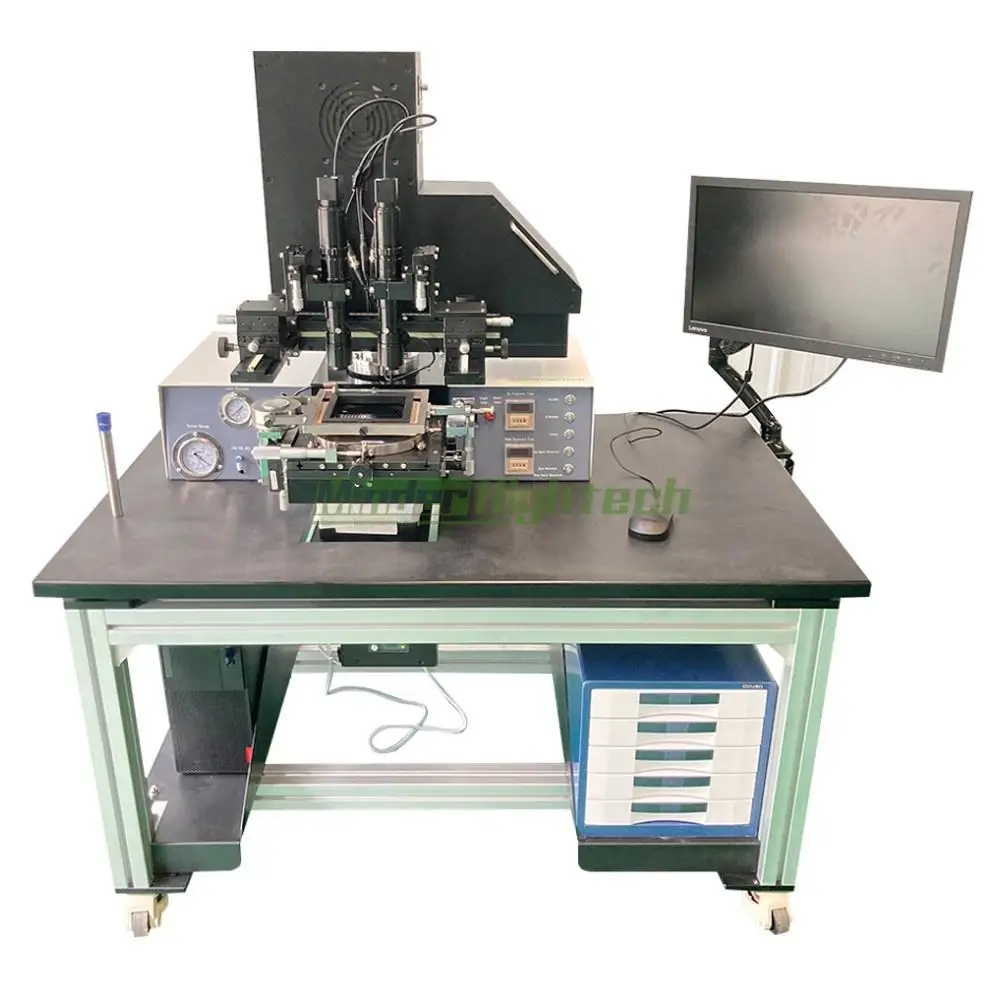
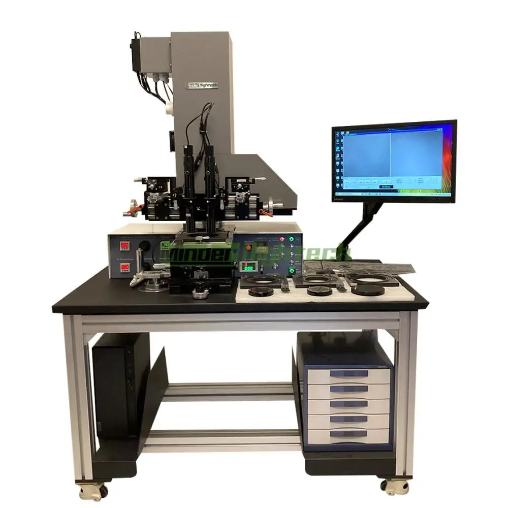
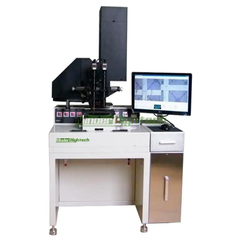
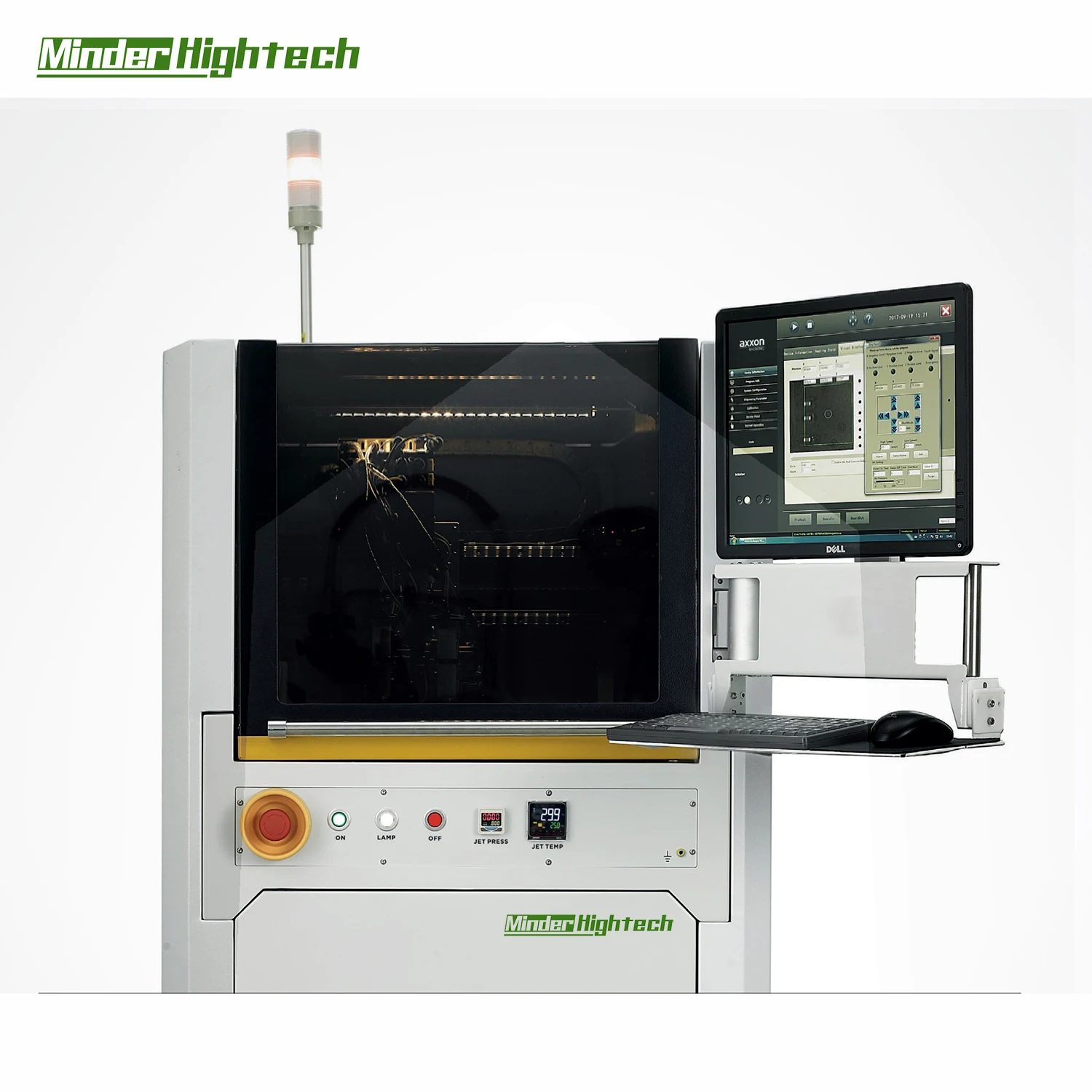
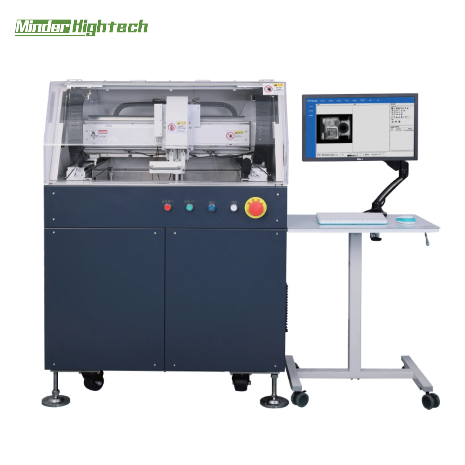
We have a mask aligner photolithography range of products, including: Wire bonder and die bonder.
Guangzhou Minder-Hightech Co.,Ltd.
Copyright © Guangzhou Minder-Hightech Co.,Ltd. All Rights Reserved
 EN
EN
 AR
AR
 BG
BG
 CS
CS
 DA
DA
 NL
NL
 FI
FI
 FR
FR
 DE
DE
 EL
EL
 IT
IT
 KO
KO
 NO
NO
 PL
PL
 PT
PT
 RO
RO
 RU
RU
 ES
ES
 SV
SV
 TL
TL
 IW
IW
 ID
ID
 LT
LT
 SR
SR
 SL
SL
 UK
UK
 VI
VI
 ET
ET
 HU
HU
 TH
TH
 TR
TR
 FA
FA
 AF
AF
 MS
MS
 GA
GA
 IS
IS
 HY
HY
 AZ
AZ
 KA
KA