
Transistor Outline (TO) is a type of transistor package designed to allow for the formation of leads and surface mounting.
As a packaged device, the ingress of dust or moisture under unsealed conditions can impair product performance, directly altering the optical path and ultimately causing malfunction. Therefore, helium mass spectrometry leak testing during production is essential, as it involves leak testing the device's seal.
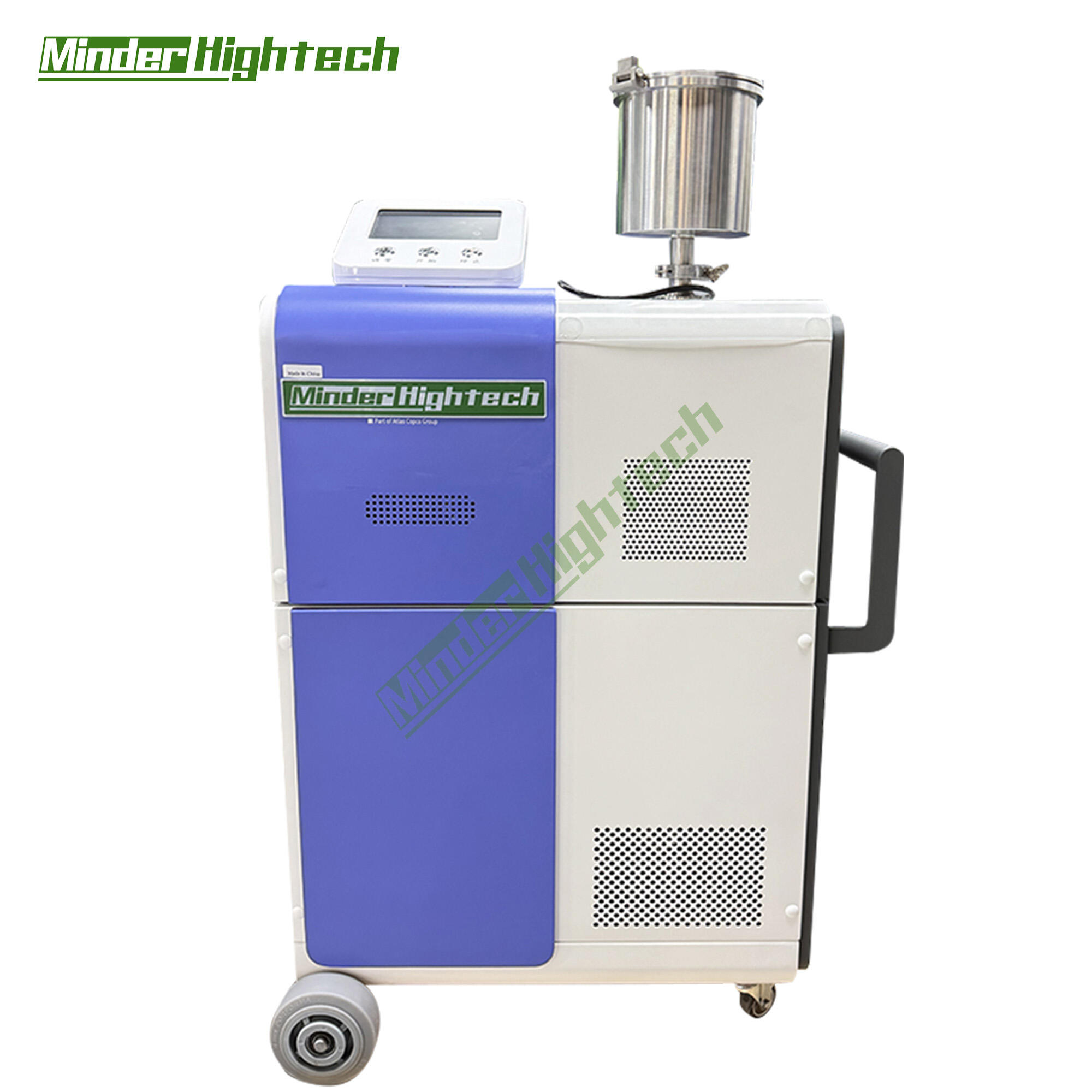
Due to the small size of packaged laser chip devices and the inability to evacuate or directly fill them with helium, TO helium mass spectrometry leak testing typically utilizes the backpressure method, a simple and reliable method. The TO packaged optical device is placed in a container at a certain pressure, and helium is introduced to compress it. After maintaining the pressure for a specified period, the device is removed and transferred to a vacuum container (leak test tank) connected to a helium detector for leak testing. Automatic testing verifies whether the device meets the package's airtightness requirements.
Guangzhou Minder-Hightech Co.,Ltd.
Copyright © Guangzhou Minder-Hightech Co.,Ltd. All Rights Reserved
 EN
EN
 AR
AR
 BG
BG
 CS
CS
 DA
DA
 NL
NL
 FI
FI
 FR
FR
 DE
DE
 EL
EL
 IT
IT
 KO
KO
 NO
NO
 PL
PL
 PT
PT
 RO
RO
 RU
RU
 ES
ES
 SV
SV
 TL
TL
 IW
IW
 ID
ID
 LT
LT
 SR
SR
 SL
SL
 UK
UK
 VI
VI
 ET
ET
 HU
HU
 TH
TH
 TR
TR
 FA
FA
 AF
AF
 MS
MS
 GA
GA
 IS
IS
 HY
HY
 AZ
AZ
 KA
KA


