
UV light source center wavelength |
405nm |
Exposure uniformity |
More than 90% |
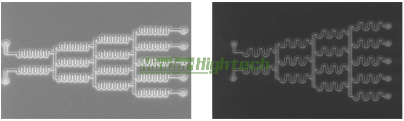
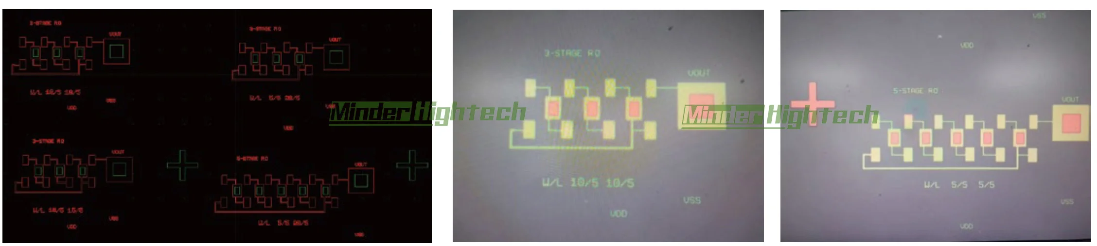
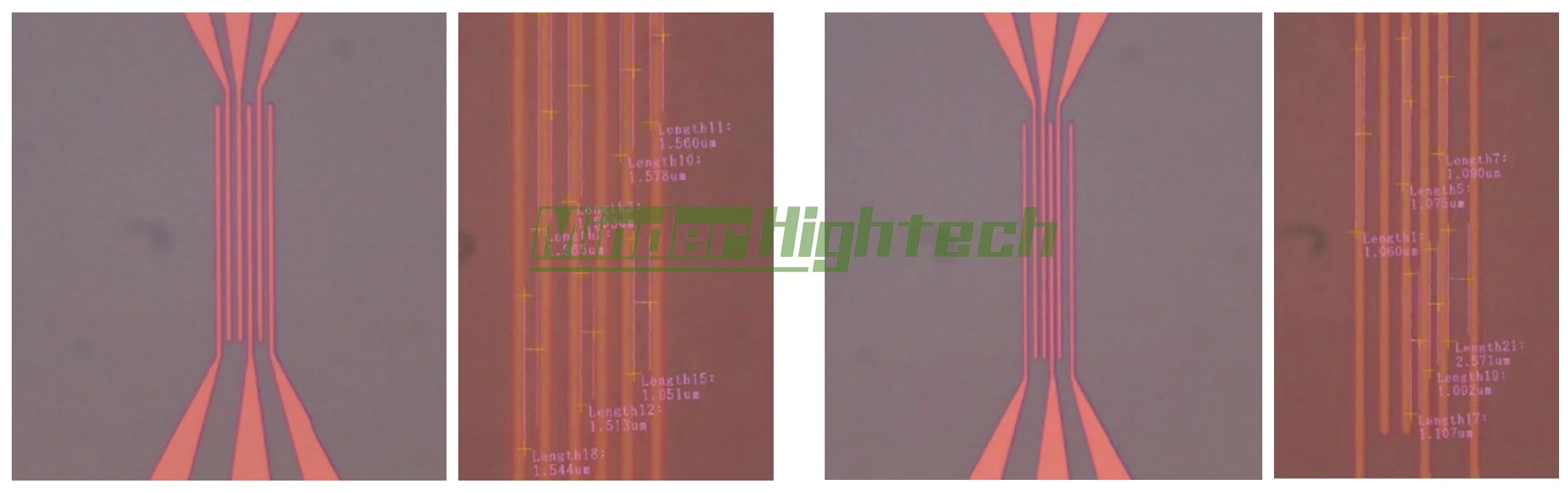
Minimum feature linewidth |
0.5um |
Single-pass writing field exposure area |
0.16*0.16mm (@0.5um) |
Writing speed |
80 mm²/min (1um feature line width) |
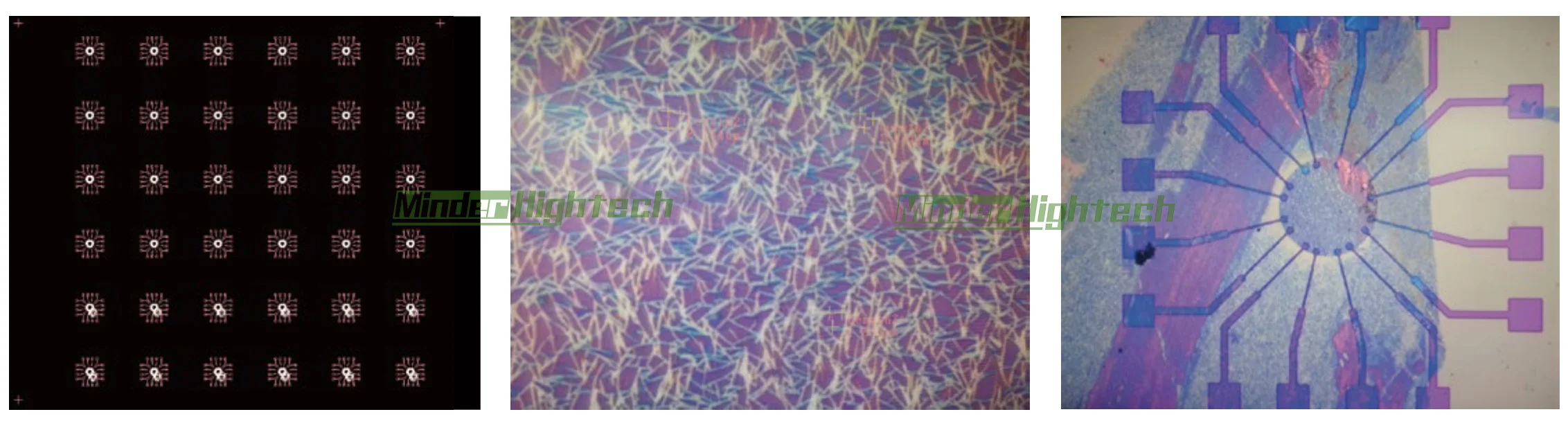
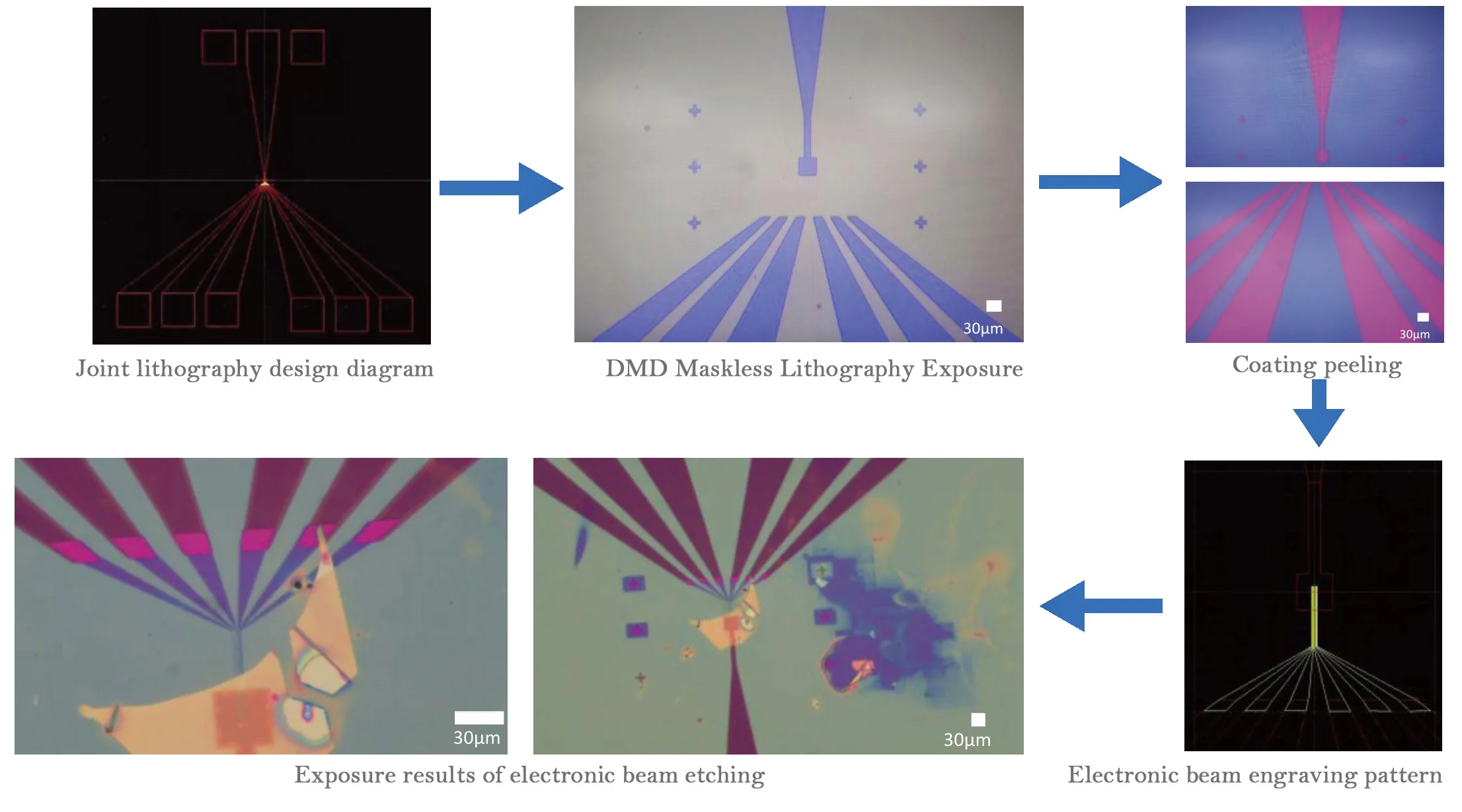
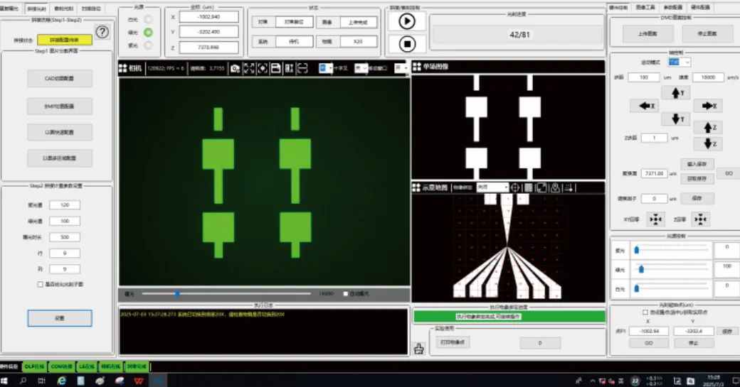
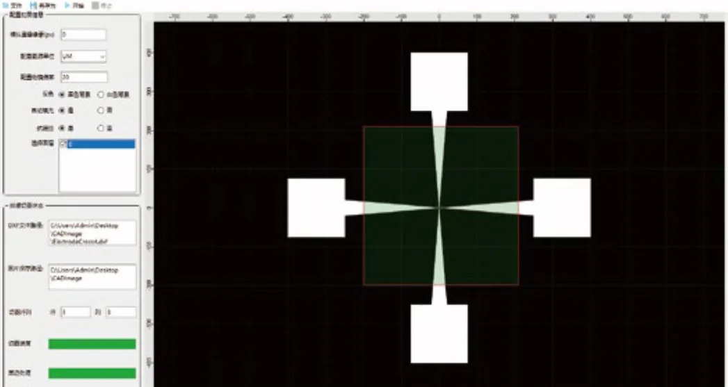
Supported image formats |
DXF, GDS, bmp, png, etc. |
Configuration |
Basic version |
Professional version |
|
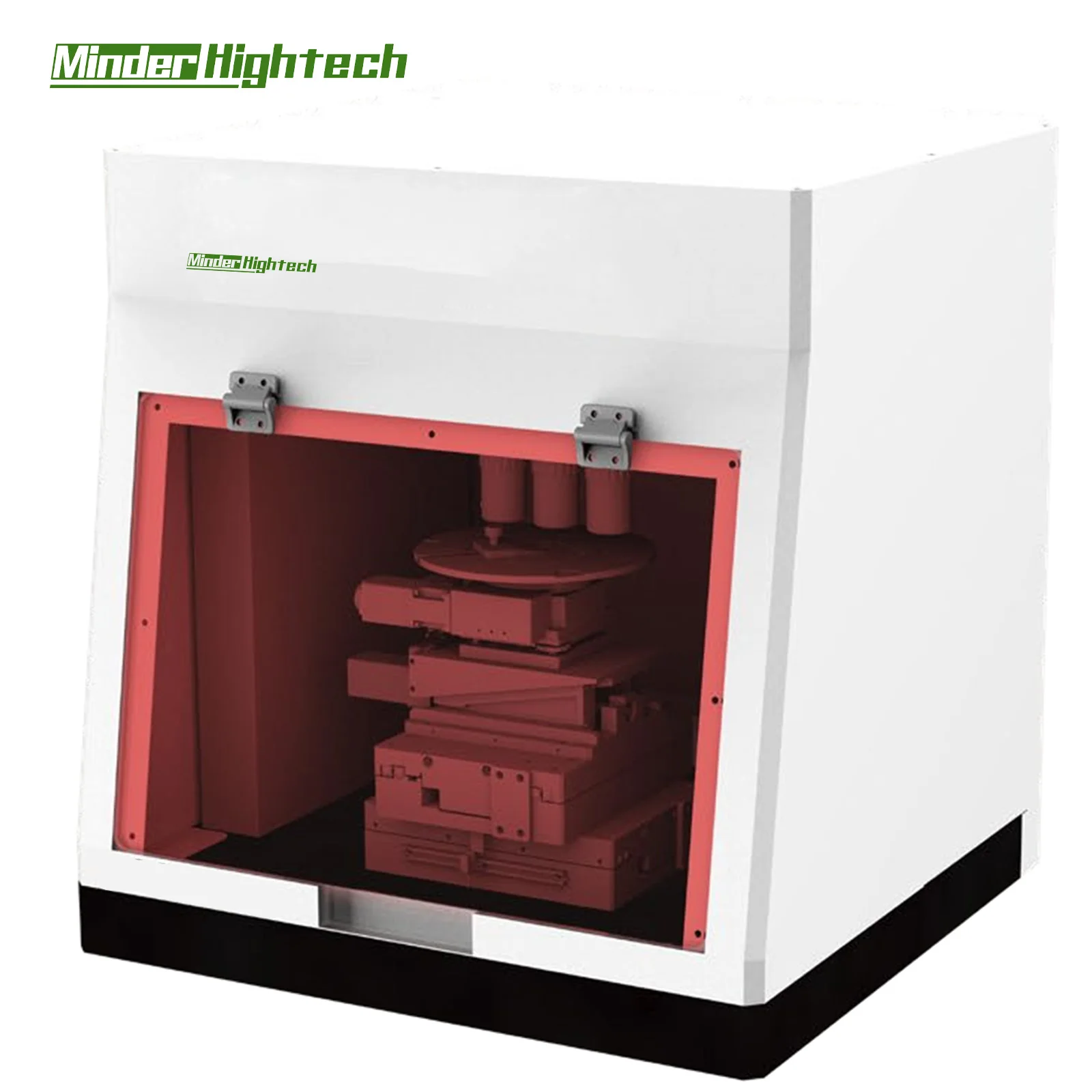
Light source |
High-power LED: 405nm |
||
DMD chip |
DLP6500 |
||
Single-field exposure area |
0.16*0.16mm (@0.5um), 0.4*0.4mm (@0.7um), 0.8*0.8mm (@1um), 1.6*1.6mm (@2um) |
||
Camera |
Large-area microscope camera (supports size measurement) |
||
Minimum equidistant line width |
0.8 µm |
0.5μm |
|
Stitching accuracy |
±0.3 µm |
±0.3μm |
|
Overlay accuracy |
±0.5 µm |
±0.5μm |
|
Writing speed |
20 mm²/min (1 µm feature linewidth) |
80 mm²/min (1μm feature linewidth) |
|
Motion stage |
High-precision linear motor (repeatable positioning accuracy ±0.25µm), leveling mechanism, manual rotary stage |
High-precision linear motor (repeatable positioning accuracy ±0.25µm), leveling mechanism, electric rotary stage |
|
Objective lens changer |
Manual objective lens switching |
Motorized objective lens switching |
|
Focusing module |
CCD image autofocus |
Laser active focusing |
|
Supported wafer sizes |
4 inch |
4-inch/8-inch |
|
Sample thickness |
0-10mm |
0-10 mm |
|


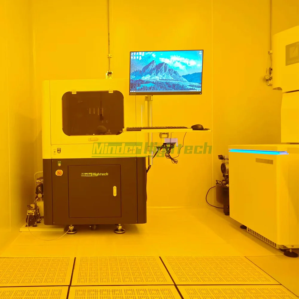
Guangzhou Minder-Hightech Co.,Ltd.
Copyright © Guangzhou Minder-Hightech Co.,Ltd. All Rights Reserved
 EN
EN
 AR
AR
 BG
BG
 CS
CS
 DA
DA
 NL
NL
 FI
FI
 FR
FR
 DE
DE
 EL
EL
 IT
IT
 KO
KO
 NO
NO
 PL
PL
 PT
PT
 RO
RO
 RU
RU
 ES
ES
 SV
SV
 TL
TL
 IW
IW
 ID
ID
 LT
LT
 SR
SR
 SL
SL
 UK
UK
 VI
VI
 ET
ET
 HU
HU
 TH
TH
 TR
TR
 FA
FA
 AF
AF
 MS
MS
 GA
GA
 IS
IS
 HY
HY
 AZ
AZ
 KA
KA