Related applications:
1. Grating etching: used for 3D display, micro-optical devices, optoelectronics, etc.;
2. Compound semiconductor etching: used for LED, laser, optical communication, etc.;
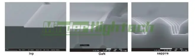
3. Patterned sapphire substrate (PSS);
4. Lithium niobate (LiNO3) etching: detectors, optoelectronics;
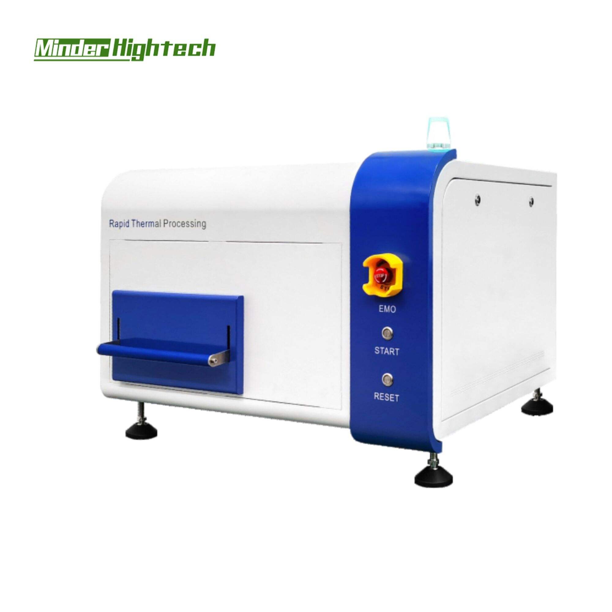
Inductively coupled reactive ion etching technology is a type of RIE. This technology achieves decoupling of plasma ion density and ion energy by independently controlling ion flux, thereby improving the control accuracy and flexibility of the etching process.
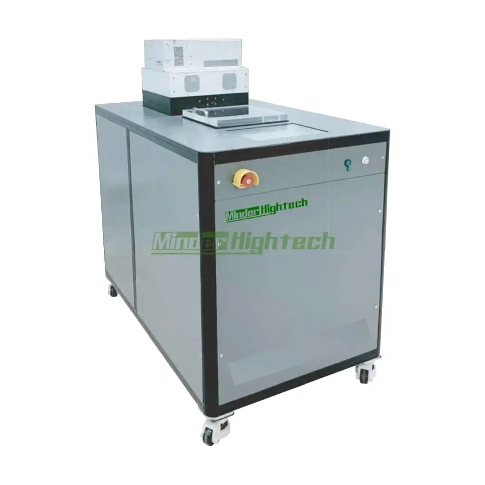
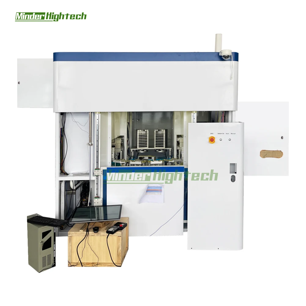
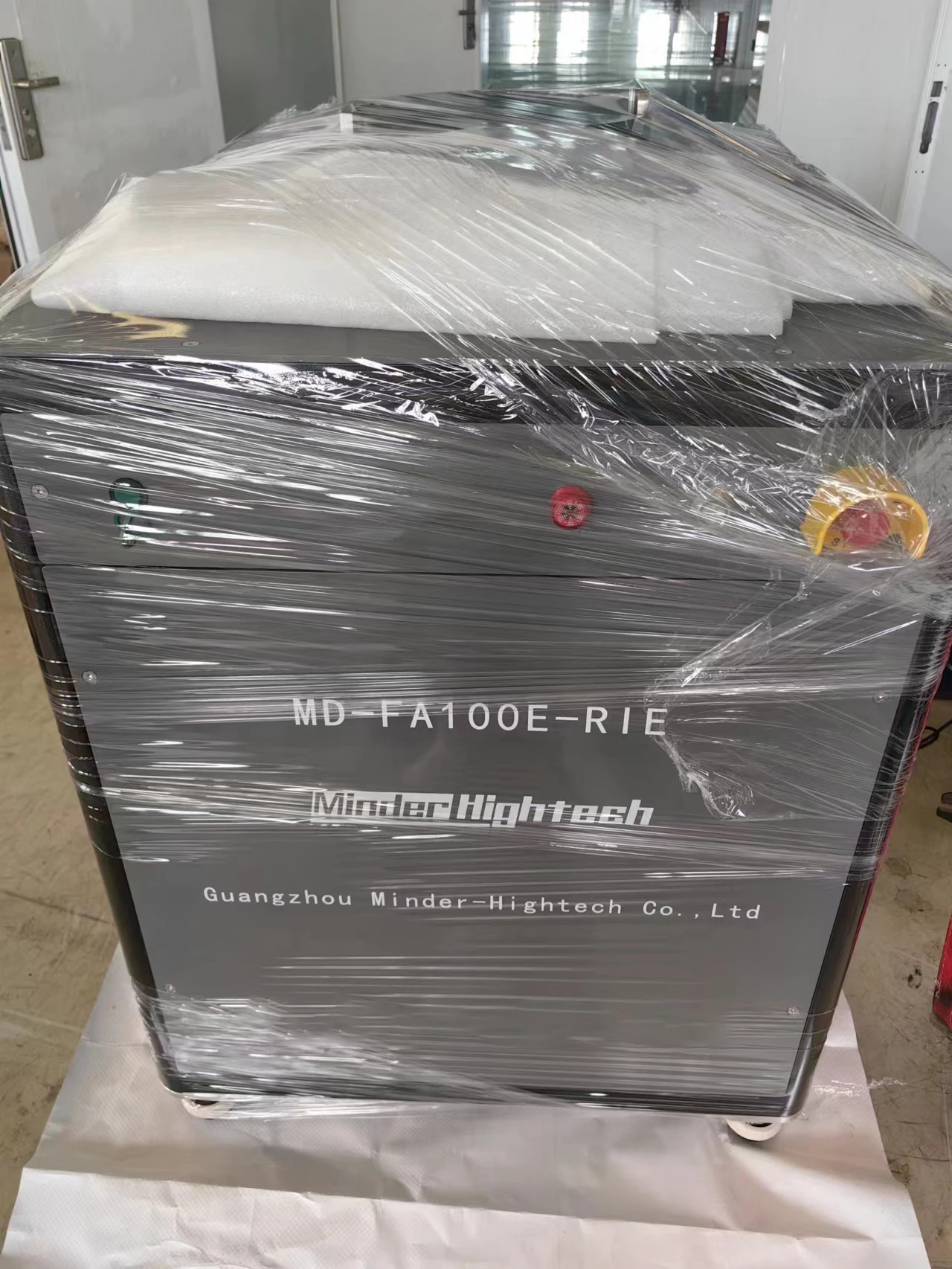
The high-density inductively coupled reactive ion etching (ICP-RIE) series products are based on inductively coupled plasma technology and are aimed at fine etching and compound semiconductor etching needs. It has excellent process stability and process repeatability, and is suitable for applications in silicon semiconductors, optoelectronics, information and communications, power devices, and microwave devices.


Applicable Materials:
1. Silicon-based materials: silicon (Si), silicon dioxide (SiO2), silicon nitride (SiNx), silicon carbide (SiC)...
2. III-V materials: indium phosphide (InP), gallium arsenide (GaAs), gallium nitride (GaN)...
3. II-VI materials: cadmium telluride (CdTe)...
4. Magnetic materials/alloy materials
5. Metal materials: aluminum (Al), gold (Au), tungsten (W), titanium (Ti), tantalum (Ta)...
6. Organic materials: photoresist (PR), organic polymer (PMMA/HDMS), organic thin film...
7. Ferroelectric/photoelectric materials: lithium niobate (LiNbO3)...
8. Dielectric materials: sapphire (Al2O3), quartz...
Related applications:
1. Grating etching: used for 3D display, micro-optical devices, optoelectronics, etc.;
2. Compound semiconductor etching: used for LED, laser, optical communication, etc.;
3. Patterned sapphire substrate (PSS);
4. Lithium niobate (LiNO3) etching: detectors, optoelectronics;
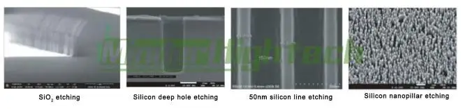
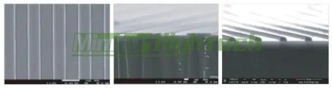
Process Result

Item |
MD150S-ICP |
MD200S-ICP |
MD150CS-ICP |
MD200CS-ICP |
MD300C-ICP |
||||
Product size |
≤6 inches |
≤8 inches |
≤6 inches |
≤8 inches |
Custom≥12inches |
||||
SRF Power source |
0~1000W/2000W/3000W/5000WAdjustable,automatic matching\,13.56MHz/27MHz |
||||||||
BRF Power source |
0~300W/0~500W/0~1000WAdjustable, automatic matching,2MHz/13.56MHz |
||||||||
Molecular pump |
Non corrosive : 600 /1300 (L/s)/Custom |
Anti-corrosion:600 /1300 (L./s)/Custom |
600/1300(L/s) /Custom |
||||||
Foreline pump |
Mechanical pump / dry pump |
Anti corrosion dry pump |
Mechanical pump / dry pump |
||||||
Pre pumping pump |
Mechanical pump / dry pump |
Mechanical pump / dry pump |
|||||||
Process pressure |
Uncontrolled pressure/0-0.1/1/10Torr controlled pressure |
||||||||
Gas type |
H2/CH4/O2/N2/Ar/SF6/CF4/ CHF3/C4F8/NF3/NH3/C2F6/Custom (Up to 12 channels, no corrosive & toxic gas) |
H2/CH4/O2/N2/Ar/SF6/CF4/CHF3/ C4F8/NF3/NH3/C2F6/Cl2/BCl3/HBr/ Custom(Up to 12 channels) |
|||||||
Gas range |
0~5sccm/50sccm/100sccm/200sccm/300sccm/500sccm/1000sccm/Custom |
||||||||
LoadLock |
Yes/No |
Yes |
|||||||
Sample tem control |
10°C~Roomtem/ -30°C~150°C /Custom |
-30°C~200°C/Custom |
|||||||
Back helium cooling |
Yes/No |
Yes |
|||||||
Process cavity lining |
Yes/No |
Yes |
|||||||
Cavity wall tem control |
No/Room tem-60/120°C |
Room tem~60/120°C |
|||||||
Control System |
Auto/custom |
||||||||
Etching material |
Silicon-base: Si/SiO2/ SiNx/ SiC..... Organic materials:PR/Organic film...... |
Silicon-base: Si/SiO2/SiNx/SiC III-V: InP/GaAs/GaN...... IV-IV: SiC II-VI: CdTe...... Magnetic material / alloy material Metallic materials: Ni/Cr/Al/Cu/Au... Organic materials: PR/Organic film...... Silicon deep etching |
|||||||
FAQ
1. About Price:
All of our prices are competitive and negotiable. The price varies depending on the configuration and customization complexity of your device.
2. About Sample:
We can provide sample production services for you, but you may provide some fees.
3. About Payment:
After the plan is confirmed, you need to pay us a deposit first, and the factory will start preparing the goods. After the equipment is ready and you pay the balance, we will ship it.
4. About Delivery:
After the equipment manufacturing is completed, we will send you the acceptance video, and you can also come to the site to inspect the equipment.
5. Installation and Debugging:
After the equipment arrives at your factory, we can dispatch engineers to install and debug the equipment. We will provide you with a separate quotation for this service fee.
6. About Warranty:
Our equipment has a 12-month warranty period. After the warranty period, if any parts are damaged and need to be replaced, we will only charge the cost price.
7. After-sale Service:
All machines have a warranty period of over one year. Our technical engineers are always online to provide you with equipment installation, debugging, and maintenance services. We can provide on-site installation and debugging services for special and large equipment.
Guangzhou Minder-Hightech Co.,Ltd.
Copyright © Guangzhou Minder-Hightech Co.,Ltd. All Rights Reserved
 EN
EN
 AR
AR
 BG
BG
 CS
CS
 DA
DA
 NL
NL
 FI
FI
 FR
FR
 DE
DE
 EL
EL
 IT
IT
 KO
KO
 NO
NO
 PL
PL
 PT
PT
 RO
RO
 RU
RU
 ES
ES
 SV
SV
 TL
TL
 IW
IW
 ID
ID
 LT
LT
 SR
SR
 SL
SL
 UK
UK
 VI
VI
 ET
ET
 HU
HU
 TH
TH
 TR
TR
 FA
FA
 AF
AF
 MS
MS
 GA
GA
 IS
IS
 HY
HY
 AZ
AZ
 KA
KA