ICP Dry Plasma Photoresist Stripper
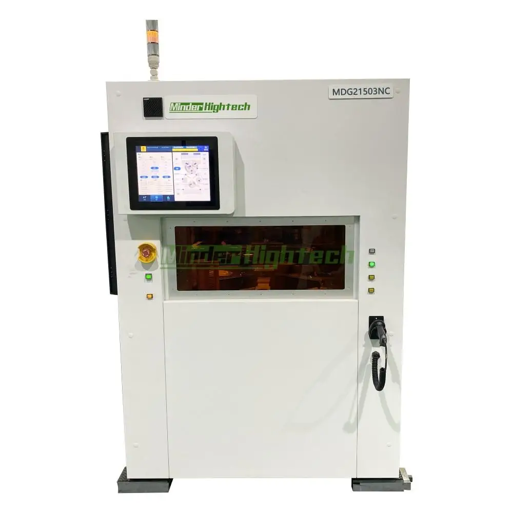
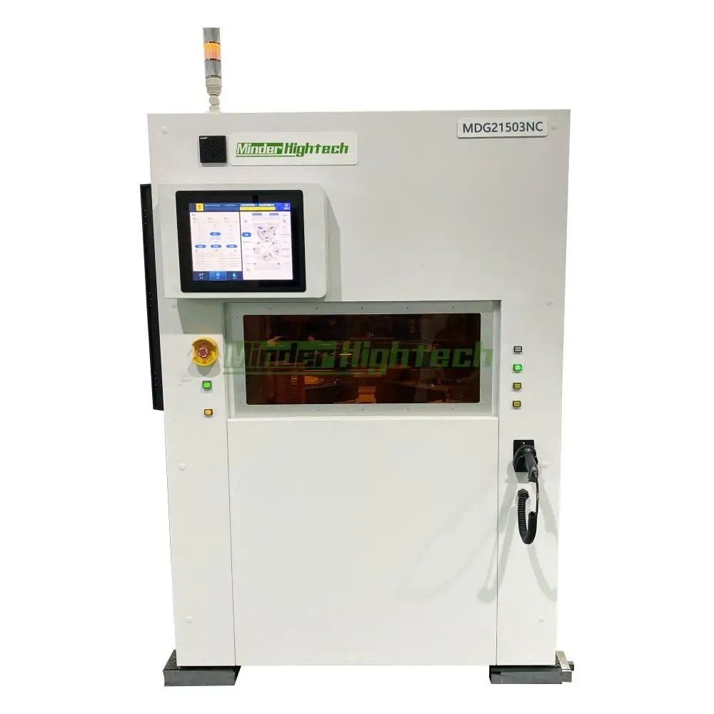
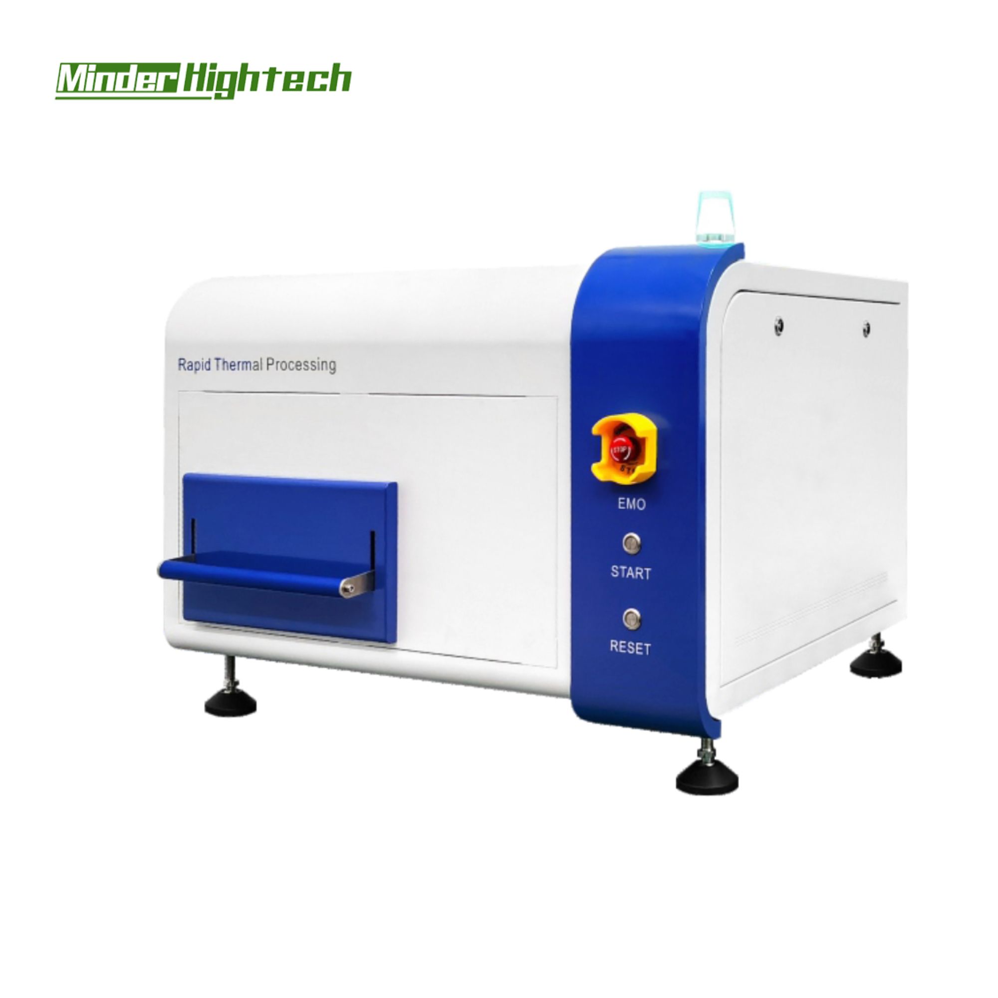
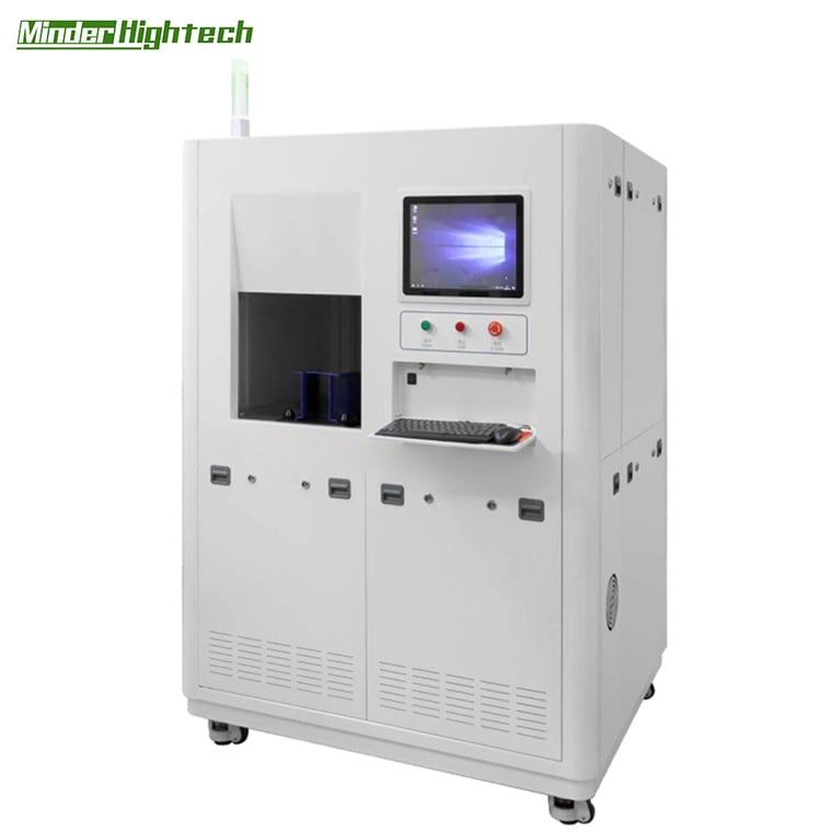
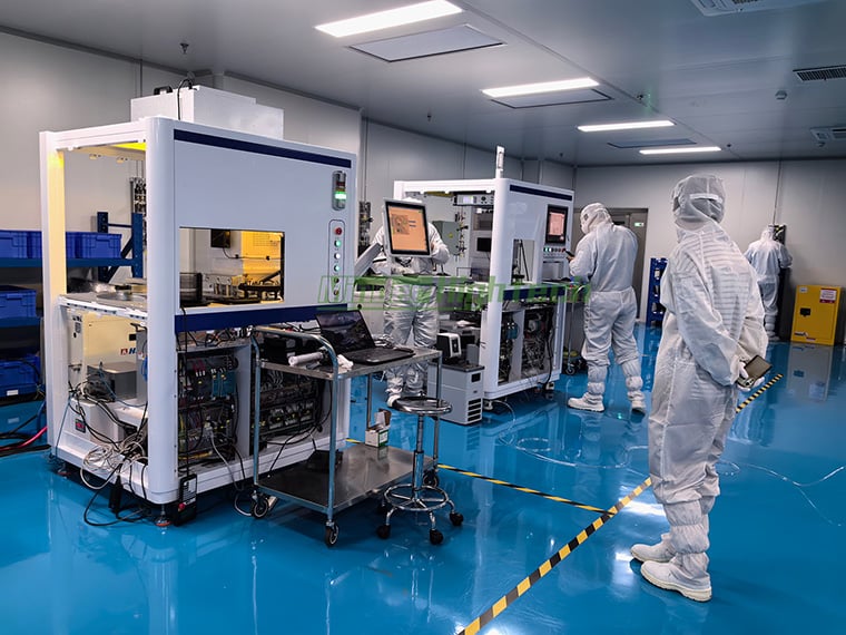
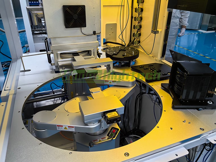
The ICP dry plasma photoresist stripper is primarily used for polymer removal, ashing, descumming, post-ion implantation photoresist removal, and the cleaning of surface residues. The MDST3100 chamber accommodates 4- to 8-inch samples with a single-wafer processing capacity, while the MDST3200 chamber accommodates 4- to 8-inch samples with a capacity of two wafers per batch.
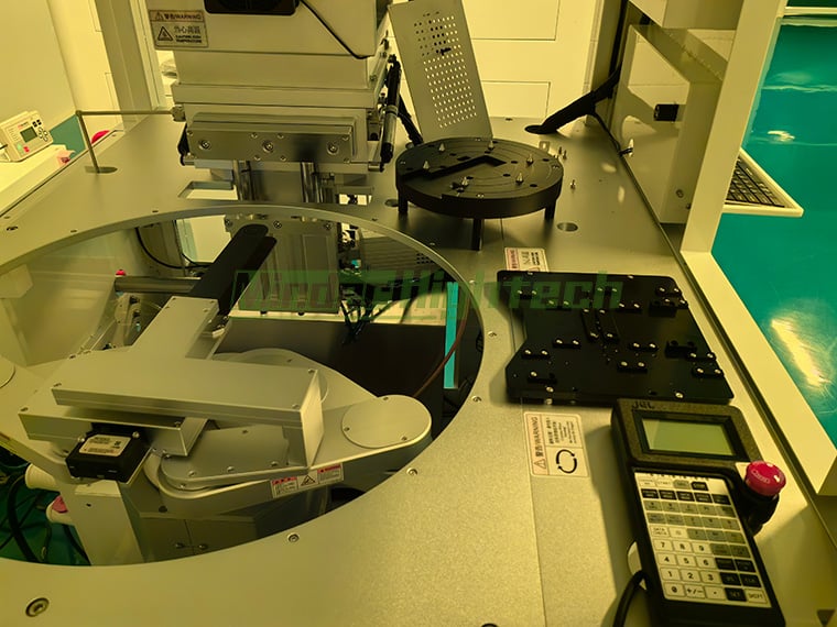
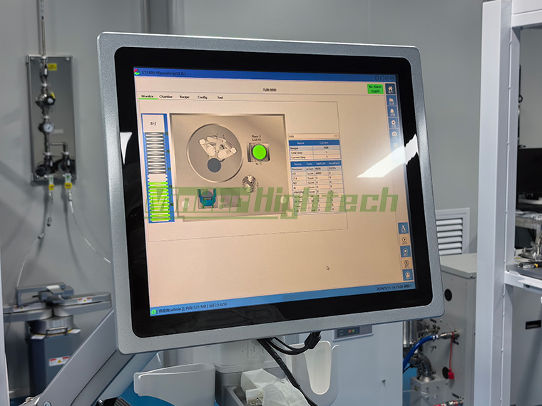
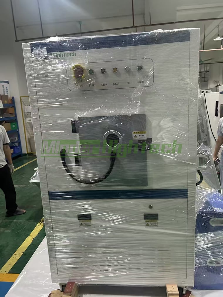
The appearance of the equipment is subject to continuous upgrades and adjustments; the actual shipped product shall prevail.
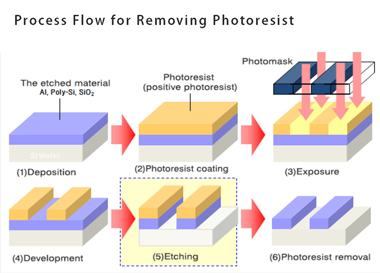
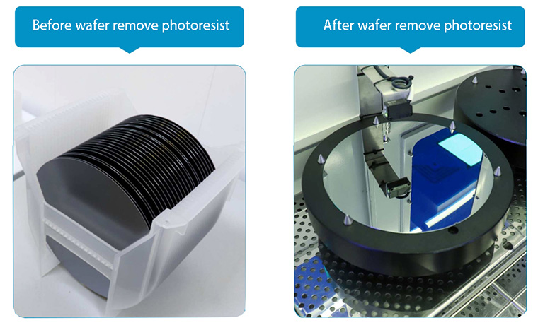
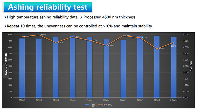
Ashing
Polymer removal
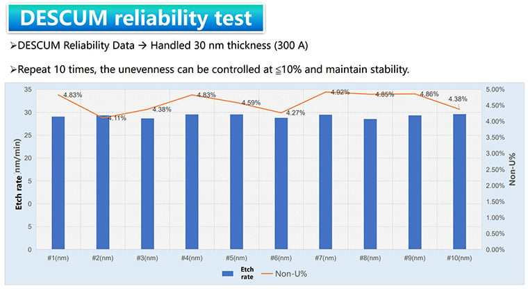
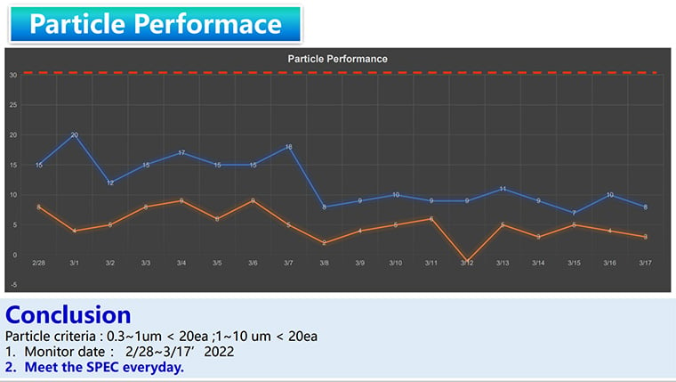
DESCUM
Dry cleaning of hard mask layer
Removal of photoresist after ion implantation
Surface residue removal
Photoresist removal in BAW/SAW process
Dry cleaning of anti-reflective graphic film layer
Surface cleaning after etching
Advantage:
High degree of plasma ionization and decomposition
After plasma treatment, the reproducibility is high
Dry etching, no pollution source
Control pressure and temperature through butterfly valves
Can maintain plasma at high pressure
Separation of High Voltage Source and Ion Generator
Microwave junction and magnetic circuit are compatible
Can meet customer requirements
Low temperature during processing
Fast response speed and short response time
Model |
MDST3100 |
MDST3200 |
|
PLASMA Source |
RF |
RF |
|
Power |
ICP |
1000W
|
1000W
|
BIAS |
NA |
NA |
|
Scope of Application |
4-8 inch |
4-8 inch |
|
Number of wafers processed in a single operation |
1 |
2 |
|
Overall Dimensions |
1300x1190x1847mm |
1300x1650x1850mm |
|
System Control |
Industrial control system |
||
degree of automation |
Automatic |
||
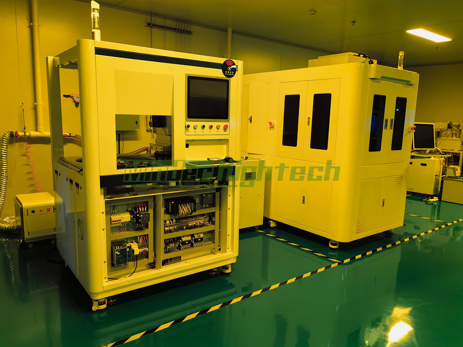
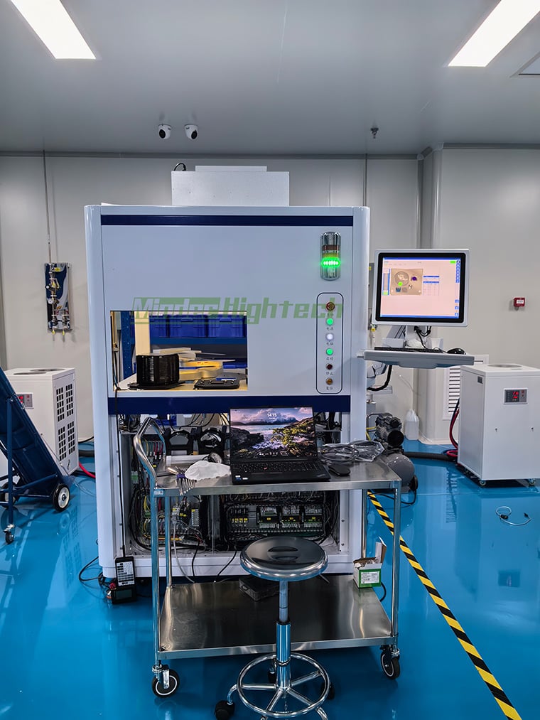
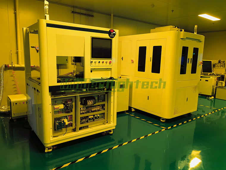
Actual Photos of Equipment:
Guangzhou Minder-Hightech Co.,Ltd.
Copyright © Guangzhou Minder-Hightech Co.,Ltd. All Rights Reserved
 EN
EN
 AR
AR
 BG
BG
 CS
CS
 DA
DA
 NL
NL
 FI
FI
 FR
FR
 DE
DE
 EL
EL
 IT
IT
 KO
KO
 NO
NO
 PL
PL
 PT
PT
 RO
RO
 RU
RU
 ES
ES
 SV
SV
 TL
TL
 IW
IW
 ID
ID
 LT
LT
 SR
SR
 SL
SL
 UK
UK
 VI
VI
 ET
ET
 HU
HU
 TH
TH
 TR
TR
 FA
FA
 AF
AF
 MS
MS
 GA
GA
 IS
IS
 HY
HY
 AZ
AZ
 KA
KA