Equipment and Technology Case Studies for High-Reliability Packaging Facilities
for Optoelectronic Devices, Uncooled Infrared Detectors, and Short-Wave Infrared Detectors
Facility Overview:
Cleanrooms (Class 1,000 / Class 10,000): R&D and mass production of infrared detectors, lasers, and MEMS gyroscopes.
The cleanrooms are equipped with advanced constant-temperature and constant-humidity HVAC systems, enabling precise environmental control to meet various circuit packaging requirements. The facility features a raised floor design and ensures excellent grounding with resistance below 4 ohms.
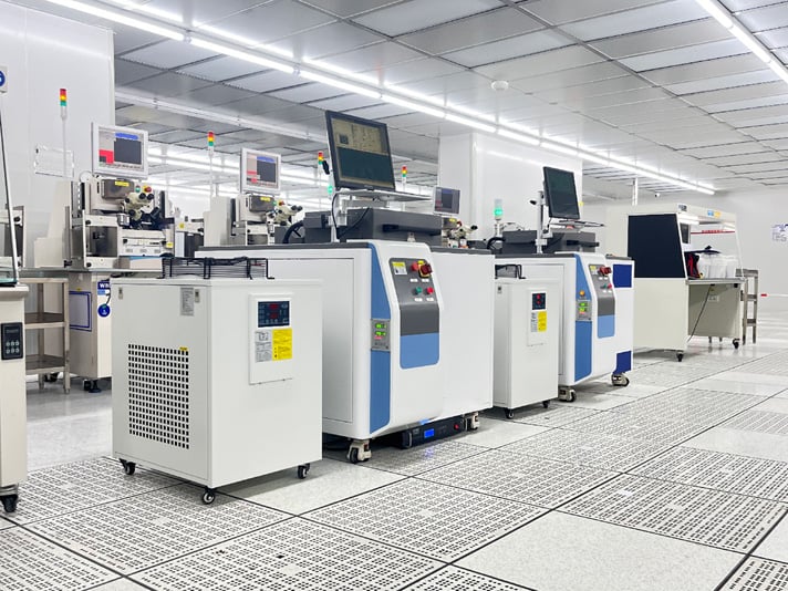
Deionized water treatment system: Achieves a resistivity of 18 MΩ·cm (at 25°C), meeting process requirements for particle levels and conductivity across various wafer cleaning specifications.
Compressed air and nitrogen generation system: Utilizes oil-free, variable-frequency screw air compressors paired with adsorption dryers, high-efficiency filters, and 99.999% purity nitrogen generators; the total content of oil mist and liquid in the gas is 0.0009 mg/m³ or less.
Packaging Process Capabilities:
Vacuum packaging production lines primarily for various models of uncooled infrared detectors have been established, capable of metal and ceramic packaging, with an annual production capacity exceeding 100,000 units.
Packaging Process Flow for Uncooled Infrared Detectors:
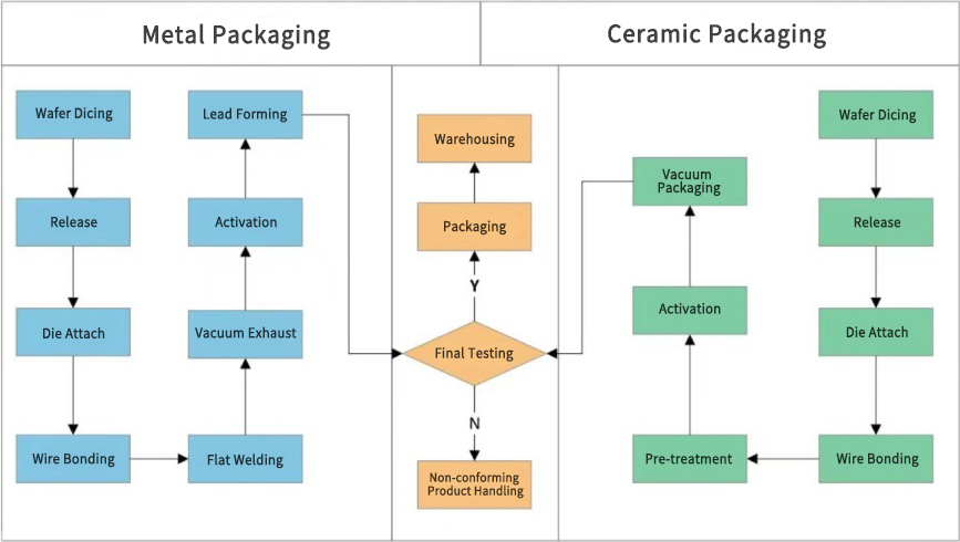
The company possesses advanced vacuum packaging technology. Key processes include DI/organic cleaning, vacuum eutectic bonding, wafer dicing, plasma-based residue removal, fully automated die bonding, semi-automated/fully automated wire bonding, high-vacuum evacuation, and vacuum encapsulation.
Cleaning: Solutions such as deionized water, acetone, and alcohol can be used to clean packaging materials and chips via immersion, rinsing, or ultrasonic cleaning.
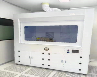
Soldering:
Utilizes a vacuum eutectic soldering process with a vacuum level of <1 Pa and an integrated formic acid-based de-oxidation module, enabling eutectic soldering with low-temperature solders at temperatures up to 450°C and achieving a void ratio of <1%; product solder joint strength is significantly enhanced through pre-soldering material treatment and optimization of the soldering process profile.
Wafer Dicing:
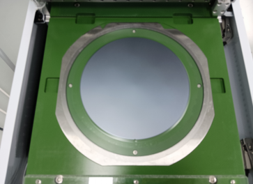
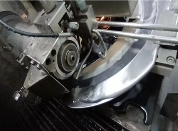
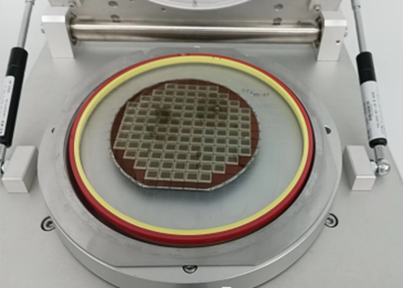
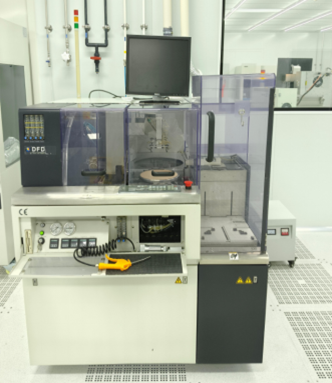
Utilizes DISCO integrated dicing and cleaning equipment, featuring fully automated dicing and cleaning capabilities. Employing both hard and soft blades, the system supports the dicing of various materials—including wafers (8 inches and smaller), glass substrates, sapphire substrates, and ceramics.
Plasma Ashing:
Utilizing advanced RF plasma processing equipment and a selection of process gases—such as N2, Ar, CF4, and O2—this process enables surface cleaning and the removal of sacrificial layers in MEMS chip structures.
Die Bonding:
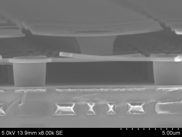
Both manual and fully automated die bonding processes are available. The manual process is suitable for rapid prototyping, utilizing a 2D optical alignment platform to maintain bonding accuracy within 50 µm. The fully automated process is designed for mass production, supporting fully automated die attach for 8-inch wafers (and smaller sizes); it accommodates die sizes ranging from 0.5 mm × 0.5 mm to 20 mm × 20 mm, allows for various epoxy dispensing pattern configurations, and achieves bonding accuracy within 30 µm.
Wire Bonding:
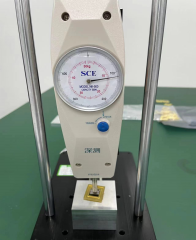
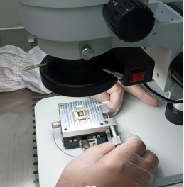
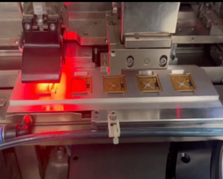
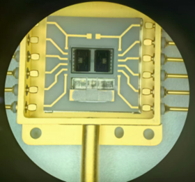
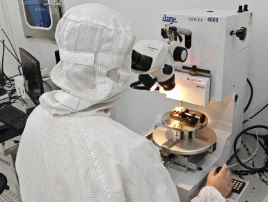
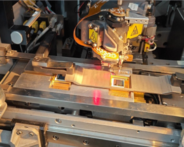
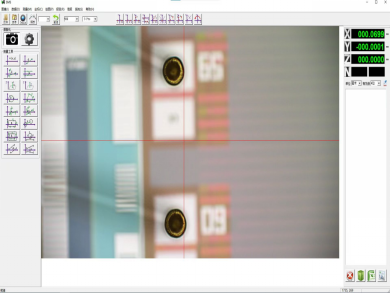
The process supports both ball bonding and wedge bonding, utilizing gold or platinum-iridium wires. It is compatible with wire diameters ranging from 20 µm to 50 µm and enables deep-cavity bonding within a depth of 25 mm. Fully automated bonding is available for gold ball bonding. Following the bonding process, wire morphology and pull strength can be measured using a measuring microscope and a pull/push tester.
High-vacuum exhaust:
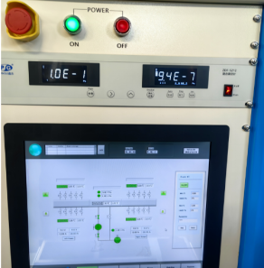
A 40-station high-vacuum exhaust system utilizing large-bore turbomolecular pumps and imported dry pumps. It achieves an ultimate vacuum of 1×10⁻⁶ Pa and a hot-state ultimate vacuum of ≤2×10⁻⁶ Pa, making it suitable for the metal packaging of uncooled infrared detectors and other devices requiring high-reliability vacuum levels.
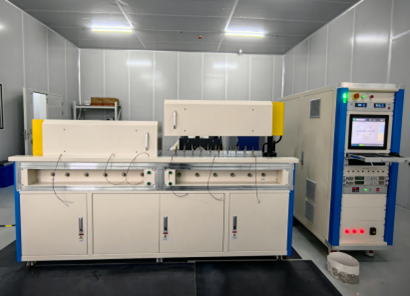
Vacuum Hermetic Packaging: Utilizes vacuum parallel seam welding or high-vacuum fusion sealing processes.
The vacuum parallel seam welding chamber is evacuated using dry pumps and cryopumps, achieving a process vacuum level of 1×10⁻⁴ Pa;
The high-vacuum fusion sealing chamber is evacuated using dry pumps and turbomolecular pumps, achieving a process vacuum level better than 5×10⁻⁵ Pa; both are suitable for the packaging of the vast majority of devices requiring high vacuum levels.
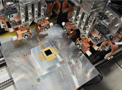
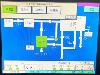
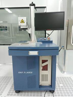
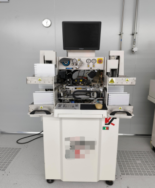
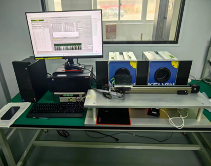
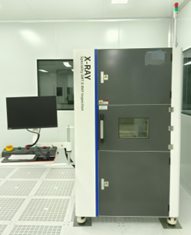
Display of selected processing equipment:
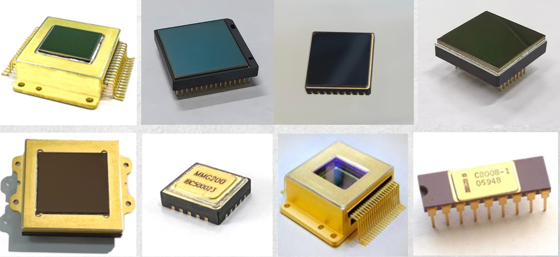
Sample Showcase:
High-Reliability Packaging for Optoelectronic Devices
Packaging for uncooled infrared detectors and short-wave infrared (SWIR) detectors, as well as metal and ceramic packaging requiring high reliability regarding hermeticity and vacuum levels. Packaging formats include CPGA, LCC, CDIP, butterfly, TO, COB, and more.
Environmental adaptability test:
A complete set of environmental adaptability testing equipment, primarily including: high and low-temperature test chambers, leak detectors, fluorinated oil platforms, vibration test benches, shock test benches, and integrated infrared parameter testing platforms.
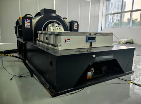
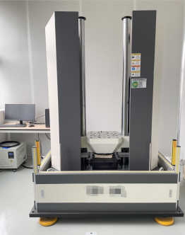
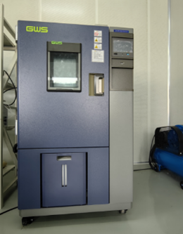
(Please contact our engineers for specific details on establishing production line equipment)
Guangzhou Minder-Hightech Co.,Ltd.
Copyright © Guangzhou Minder-Hightech Co.,Ltd. All Rights Reserved
 EN
EN
 AR
AR
 BG
BG
 CS
CS
 DA
DA
 NL
NL
 FI
FI
 FR
FR
 DE
DE
 EL
EL
 IT
IT
 KO
KO
 NO
NO
 PL
PL
 PT
PT
 RO
RO
 RU
RU
 ES
ES
 SV
SV
 TL
TL
 IW
IW
 ID
ID
 LT
LT
 SR
SR
 SL
SL
 UK
UK
 VI
VI
 ET
ET
 HU
HU
 TH
TH
 TR
TR
 FA
FA
 AF
AF
 MS
MS
 GA
GA
 IS
IS
 HY
HY
 AZ
AZ
 KA
KA