A process of using special chemicals to selectively remove the top portion of a material called photoresist. The so-called photoresist is a light-activated sticky material. The altered properties of photosensitive material offer the ability to form unique shapes and designs during light exposure. This way we can produce readable, high-definition designs on the face of an electronic device — information that it needs to have if its going to work.
An etchant is applied during photoresist etch back process. When this etchant comes in contact with the photoresist material it basically eats some of the outer layer where we want to keep and get rid of —our pattern. This is useful in the case shapes that a different heights like multiple levels. This enables us to build intricate designs necessary for high-tech.
There are a number of key advantages to using photoresist etch back for electronics applications. Primarily, it creates incredibly precise pattern work. Since an error in one of the patterns could result in issues with how a device operates, it is important that this step be very accurate. If the designs are even a little off then they ill result in none of the device to function as intended. These errors are mitigated by the photoresist etch back process which generates precise and accurate features suitable for implementation in wafers.
Not only does this increase accuracy, but it also improves a thing called the aspect ratio. Aspect Ratio — Aspect ratio is the relationship between an object's height and width. If we remove the layers of photoresist material above carefully then we can increase its aspect ratio without damaging other successive layer. The evolution makes it easier to create even more complex shapes needed for creating next-generation computer chips and other electronic devices.
Photoresist Downstream Ashing in Electronic Device Manufacturing This facilitates patterning the various devices in a computer chip, or any other electronic component. This makes possible creation of the minute and complex designs that are essential for various advanced operations used in modern technology. This is what makes them capable of performing complex tasks and doing everything we can get our little hands on.
There are ways to ensure optimum utilization of photoresist etch back for maximum benefits. Multiple Coats of PhotoresistAnother common practice is to use multiple coats of photo resist. In this way we make a longer layer able to withstand the process of attacking and etching with chemicals. In addition to that, photoresist thickness variation may yield the gentle slope in patterns. This in turn can further improve the aspect ratio of final patternsFile But not limited only to speeding up, or compressing the pattern slopes.
For the development of advanced computer chips and related components, this technique called photoresist etch back is very critical. This process also allows for smaller and more complicated patterns to be made on the chip surface. Building the tiny circuits that chips require to work is helped a great deal by just how intricate these designs must be. And with the evolution of technology, designing such designs becomes even more important.
Minder Hightech comprises a team of highly educated engineers, professionals, and staffs with outstanding expertise and experience. Our brand's products have spread to major industrialized countries across the globe aiding customers to improve efficiency, Photoresist etch back and increase the quality of their products.
Minder-Hightech is now a very Photoresist etch back brand in the industrial world, based on many years of experience in machine solutions and good relationship with oversea customers of Minder-Hightech, we created "Minder-Pack" which focuses on the machinery on packages solution as well as other high-value machines.
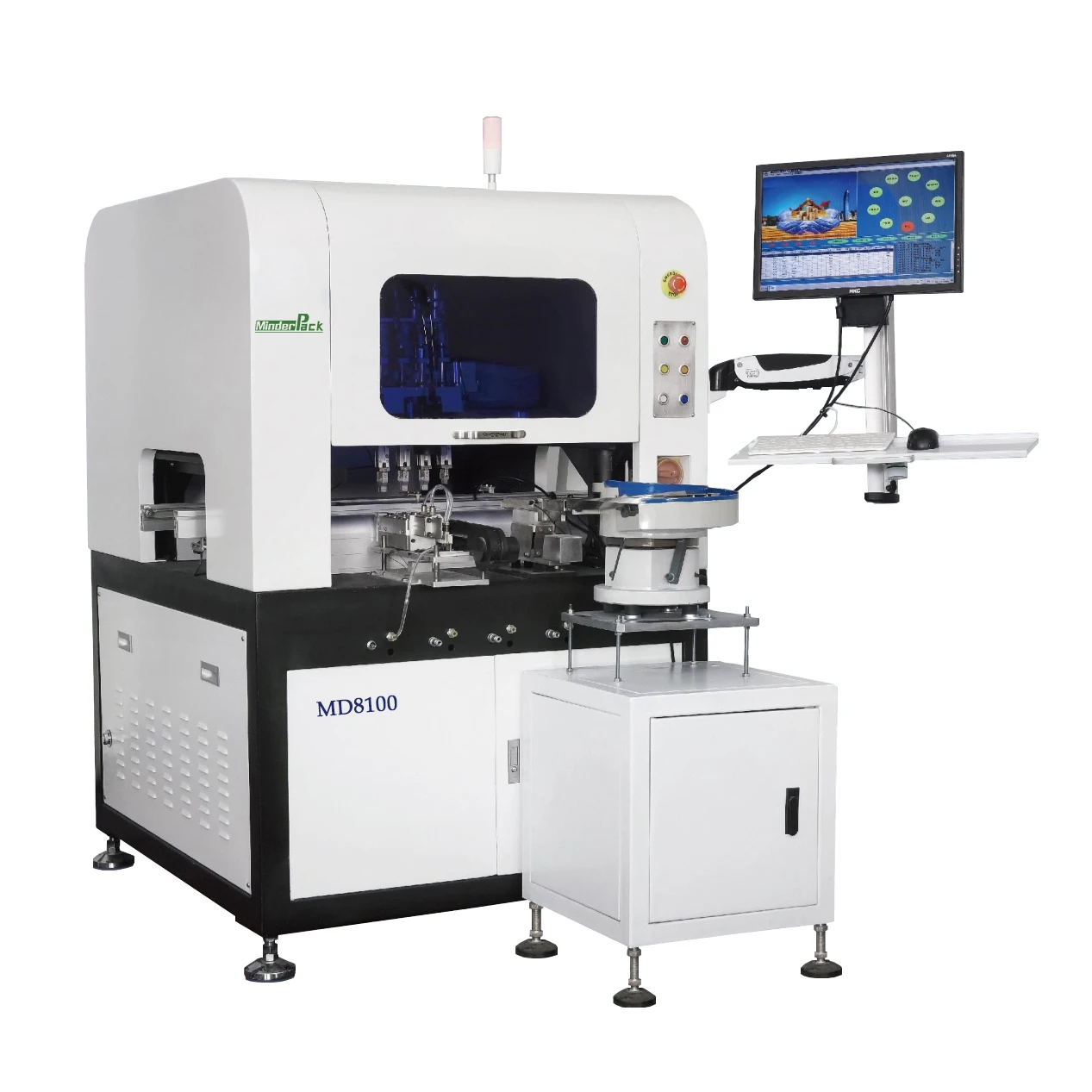
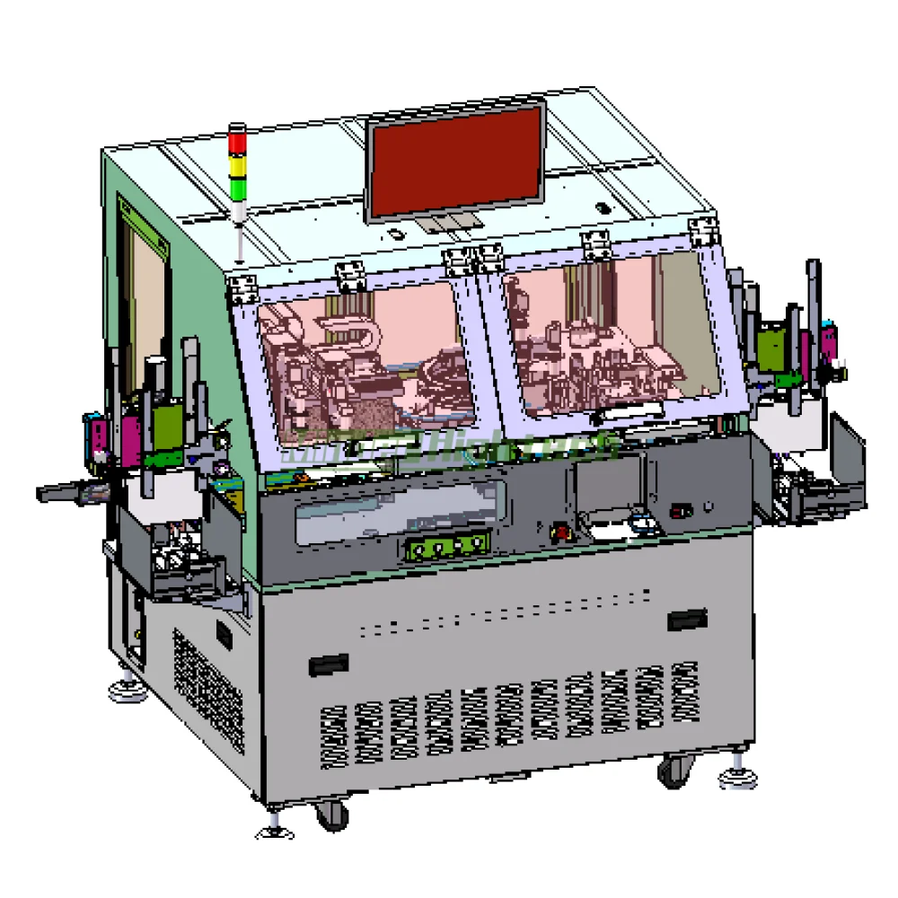
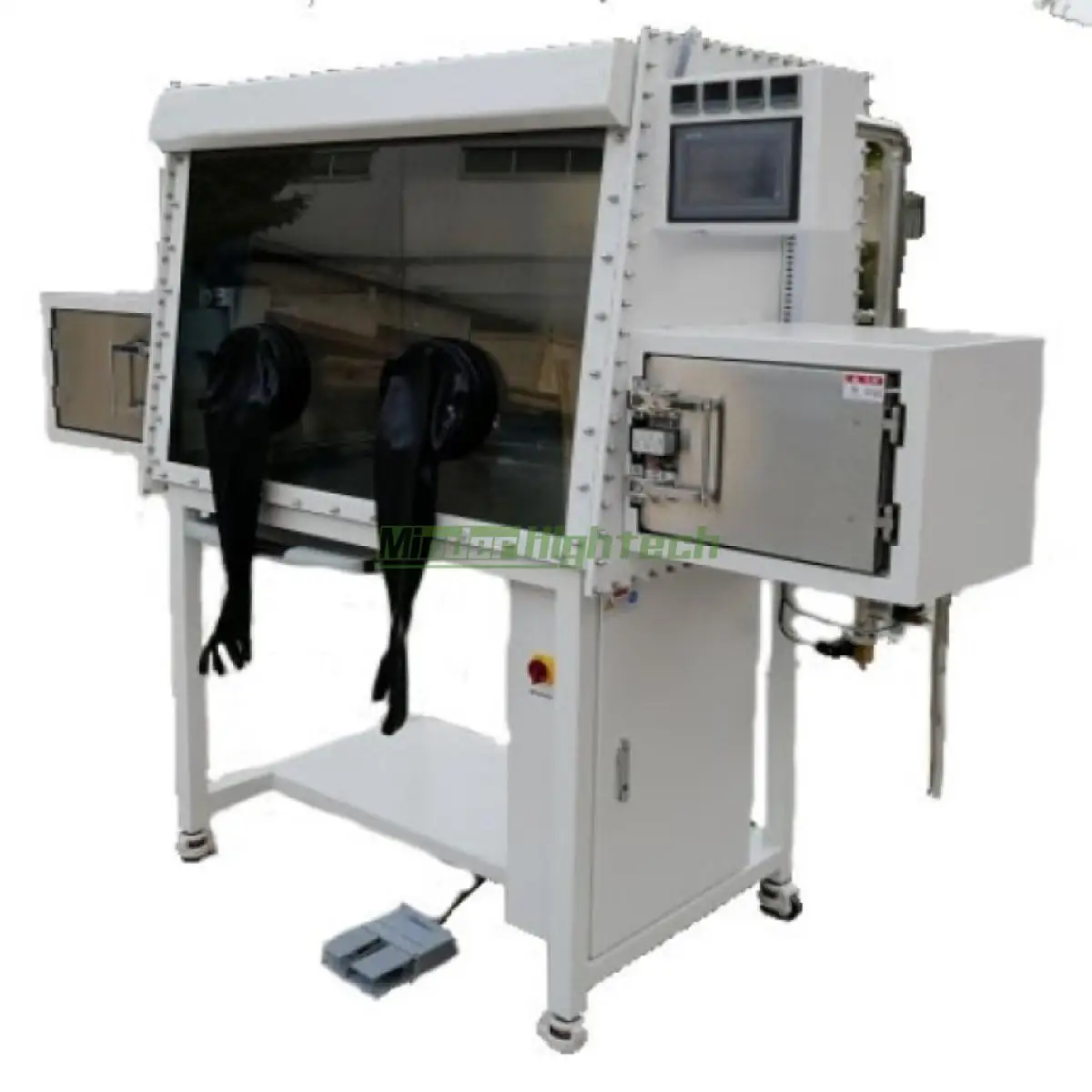
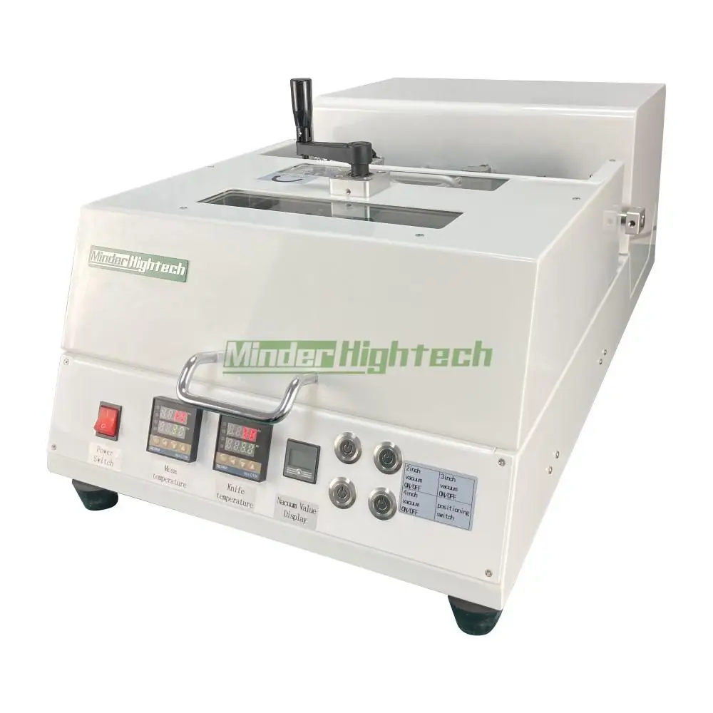
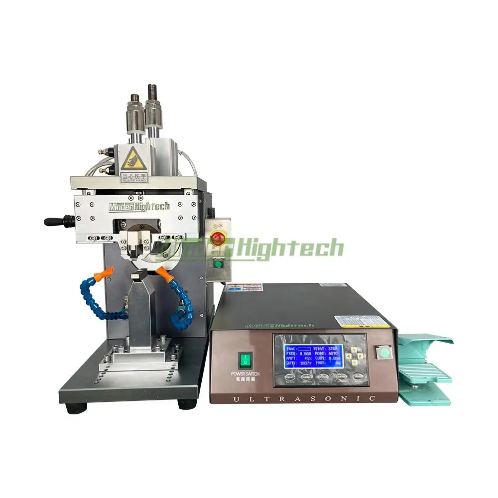
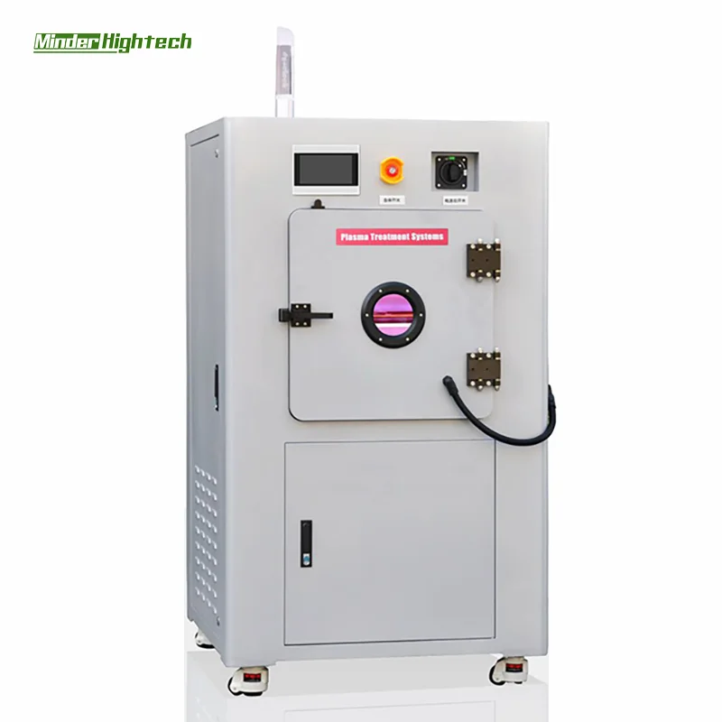
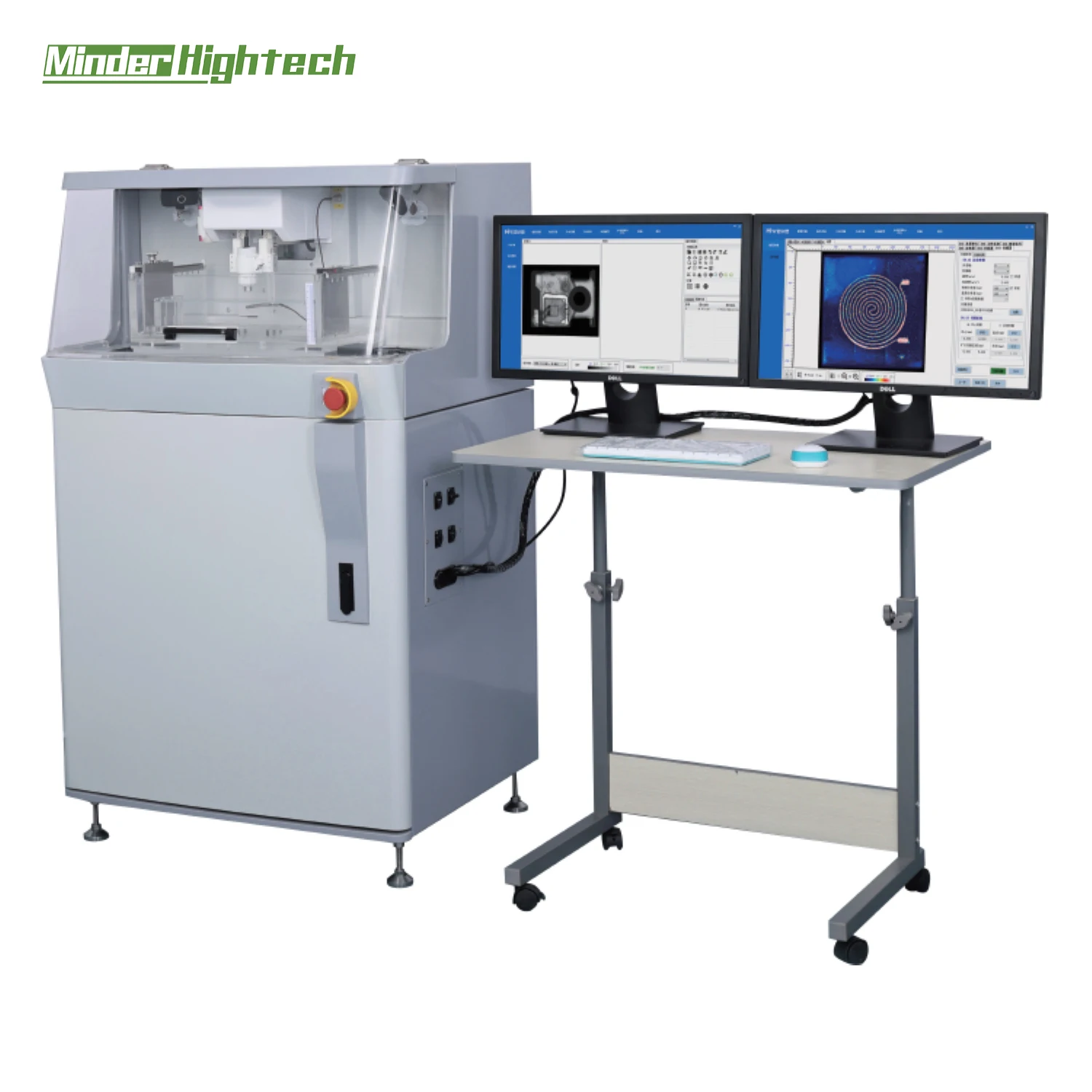
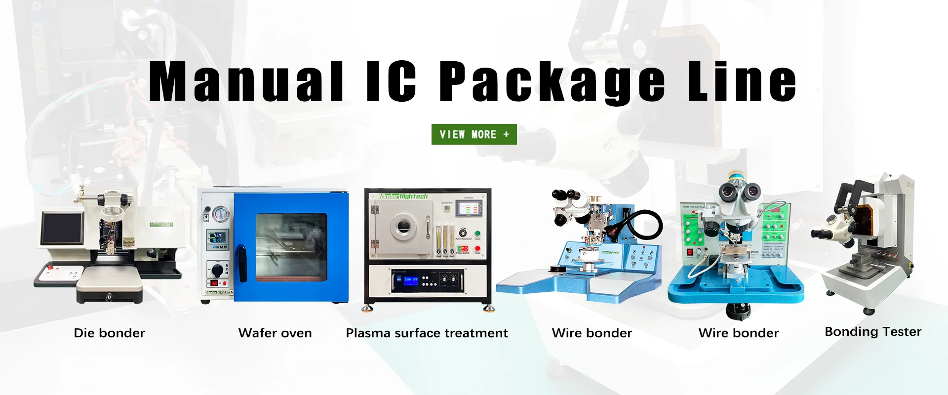
We offer a Photoresist etch back range of products, including wire bonder and die bonder.
Minder-Hightech represents the semiconductor as well as electronic products industry in sales and service. Our equipment sales experience spans 16 years. The company is committed to offering customers Photoresist etch back, Reliable, and One-Stop Solutions for machinery equipment.
Guangzhou Minder-Hightech Co.,Ltd.
Copyright © Guangzhou Minder-Hightech Co.,Ltd. All Rights Reserved
 EN
EN
 AR
AR
 BG
BG
 CS
CS
 DA
DA
 NL
NL
 FI
FI
 FR
FR
 DE
DE
 EL
EL
 IT
IT
 KO
KO
 NO
NO
 PL
PL
 PT
PT
 RO
RO
 RU
RU
 ES
ES
 SV
SV
 TL
TL
 IW
IW
 ID
ID
 LT
LT
 SR
SR
 SL
SL
 UK
UK
 VI
VI
 ET
ET
 HU
HU
 TH
TH
 TR
TR
 FA
FA
 AF
AF
 MS
MS
 GA
GA
 IS
IS
 HY
HY
 AZ
AZ
 KA
KA