 EN
EN
 AR
AR
 BG
BG
 CS
CS
 DA
DA
 NL
NL
 FI
FI
 FR
FR
 DE
DE
 EL
EL
 IT
IT
 KO
KO
 NO
NO
 PL
PL
 PT
PT
 RO
RO
 RU
RU
 ES
ES
 SV
SV
 TL
TL
 IW
IW
 ID
ID
 LT
LT
 SR
SR
 SL
SL
 UK
UK
 VI
VI
 ET
ET
 HU
HU
 TH
TH
 TR
TR
 FA
FA
 AF
AF
 MS
MS
 GA
GA
 IS
IS
 HY
HY
 AZ
AZ
 KA
KA
/images/share.png)
Ach an éisteann tú le ceist: cad is iad micscrópáin scaneála fuinneamhacha? Bíonn na n-inneall beaga seo ag athrú conas déantar dochtú ar phroducta ag fiontrachóga. Féachaimid anois conas tá micscrópáin scaneála fuinneamhacha ag athrú an modh atá ag na gcomhlachtaí seo chun a gcuid phroduct a reic.
Conas Tugann Micscrópáin Scaneála Fuinneamhacha Cabhrú
Tá na gcomhlachtaí fiontrachóga ag lorg beartas níos fearr chun a gcuid phroduct a sheiceáil. Úsáidtear micscrópáin scaneála fuinneamhacha acu chun isteach san phríomhphobal is lú de a gcuid phroduct. Is eolaíocht bhailithe ar thuinntheacha fuinneamh é, a chruthaíonn íomhánna soiléir de mhodhnaithe fiontrachóga. Tabharfaidh sé cabhair donn chomhlachtaí locáil pléaráin a d'fhéadfadh cóiriú ar chothromlacht a gcuid phroduct.
Fuinneamhach: Athrú ar Níos Fearr ar Phrós Feabhsuithe
Is féidir le microscópaí scannála uillteach fíorshaol a chur ar fáil do chuigpháirtithe chun an rialú gairide a bhaint amach go níos hiomlán. Is cinnte go dtabharfar faoi deara na probléimeanna go luath chun go mbeidh na cuigpháirtithe ag feabhsú ar dhéanamh an fearr as a n-áirítear. Ní hé sin ach go dtiocfaidh sé chun fíortharraingt na n-earraí sólidstaiti a fheabhsú, ach bíonn sé chomh baineach le cúplaíocht agus ama a thabhairt amach gan na hábhar éagsúla a shuíomhú síos.
Níos Tapaigh agus Níos Fíorshuim
Chuaigh Cruz ina chónaí chomh maith le cuigpháirtithe eile ag Bainistíocht Fhiar Ulltrabheo comhionann a n-earraí go níos tapa agus go níos fíor. Le réamhamharc níos tapa ar chuid den scagaire agus íomhái clár, is féidir le buachaillí comhlacht a phointe earráide a aimsiú agus a chur i gcás. Is féidir leo seo a dhéanamh go níos hiomlán agus cóstaí phróiseála a laghdú trí blianta.
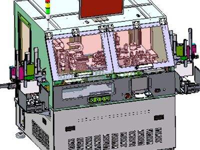
Minder-Hightech Solutions
Is féidir le hiomparaitheoirí smicléachta a bhfuil intinn acu a n-ardú faoi mar a bheidh fiontra ó na freastalaithe scanála rófhréamhaithe ag Minder-Hightech. Tabharfaidh ár théicneolaíocht bréige cabhrach do chuideacha chun ceartlann an phríomhsacar a n-inspéid nó go mbeidh siad ag úsáid na n-ábhar is fearr amháin. Is féidir le cuideachta scandaí a fháil ar chóip agus cúnamh éifeachtach a thabhairt do na pródachtaí leo trína n-úsáid de na miscrópaí sceanaigh rófhréamhaithe againn.
Rátaí Níos Airde i gCás an Smicléachta
Tacaíonn ceisteacha rófhréamhaithe le cuideachta diobhthuithe a aimsiú sa chéad staid agus a n-athraíonn a gcuid pròiseasanna fainneogaireachta i gcoitinne. Ní amháin go dtiocfaidh sé seo le cúram na n-ábhar smicléachta a fheabhsú ach go mbeidh sé ag tabhairt cúnamh do chuideacha airgead a shábháil sna blianta chugainn.
Mura ndéanann tú seiceáil don gach imeacht, Bonnlón Másc ag plé leis an gcostas den chur isteach ar chóras nó léiriúchán ardaithe, nó ag dul i ngleic le cúram miondétachta? Úsáid an eolais seo chun cuideachtaí a shábháil trí fheabhsú ar an bhfheabhsanacht, mar aon le déileáil níos gairid agus níos príobháideach, agus taithí níos fearr. Le taithí fíorfhocalach, tá Minder-Hightech i gcás maith chun freastal ar phriomhtheangacha nuálacha do scannáir mhicroscóp éadrom leictreach don seola semi-chonduchtora a díriú ar fheabhsú ar an gceartú atá acu. Cuirimid béim ar chomhlámha is fearr a úsáid agus sin a chur in iúl don spás semi-chonduchtora chun feabhsú níos fearr agus níos hiomlán.


